Description
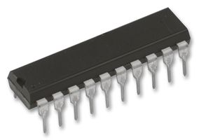
HYUNDAI/HYNIX HY6264ALP-10 Standard Static RAM, 8Kx8, 28 Pin, Plastic, DIP
DESCRIPTION
The HY6264ALP-10 is a high-speed, low power and 8,192×8-bits CMOS static RAM fabricated using Hyundai’s high performance twin tub CMOS process technology. This high reliability process coupled with innovative circuit design techniques, yields maximum access time of 70ns. The HY6264A has a data retention mode that guarantees data to remain valid at the minimum power supply voltage of 2.0 volt. Using the CMOS technology, supply voltage from to 5.5 volt has little effect on supply current in the data retention mode. Reducing the supply voltage to
FEATURES
· Fully static operation and Tri-state outputs TTL compatible inputs and outputs Low power consumption Battery backup(L/LL-part) -2.0V(min.) data retention· Standard pin configuration -28 pin 600 mil PDIP -28 pin 330 mil SOP
Product Voltage Speed No. (V) (ns) 5.0 70/85/100 Note 1. Current value is max.
A0 SENSE AMP ROW DECODER ADD INPUT BUFFER I/O1 OUTPUT BUFFER I/O8
Pin Name /CS1 CS2 /WE /OE A0-A12 Pin Function Chip Select 1 Chip Select 2 Write Enable Output Enable Address Inputs Pin Name I/O1-I/O8 Vcc Vss NC Pin Function Data Input/Output Power(+5V) Ground No Connect
This document is a general product description and is subject to change without notice. Hyundai Electronics does not assume any responsibility for use of circuits described. No patent licenses are implied. Rev.02 /Jan.99 Hyundai Semiconductor
PART NO. HY6264ALJ HY6264ALLJ SPEED POWER L-part LL-part L-part LL-part PACKAGE PDIP SOP
Symbol Vcc, VIN, VOUT TA TSTG PD IOUT TSOLDER Parameter Power Supply, Input/Output Voltage Operating Temperature Storage Temperature Power Dissipation Data Output Current Lead Soldering Temperature & Time Rating -65 to Unit W mA °C·sec
Note 1. Stresses greater than those listed under ABSOLUTE MAXIMUM RATINGS may cause permanent damage to the device. This is stress rating only and the functional operation of the device under these or any other conditions above those indicated in the operation of this specification is not implied. Exposure to the absolute maximum rating conditions for an extended period may affect reliability.
TO 70°C Symbol Parameter Vcc Supply Voltage VIH Input High Voltage VIL Input Low Voltage Min. 2.2 -0.5(1) Typ. 5.0 Max. Vcc+0.5 0.8 Unit V
/CS1 CS2 /WE /OE MODE Standby Output Disabled Read Write I/O OPERATION High-Z Data Out Data In
Vcc to 70°C (Normal) unless otherwise specified Symbol Parameter Test Condition ILI Input Leakage Current Vss < VIN < Vcc ILO Output Leakage Current Vss < VOUT < Vcc CS2=VIL or /OE = VIH or/ WE = VIL Icc Operating Power Supply /CS1 = VIL, CS2=VIH, Current VIN = VIH or VIL, II/O 0mA ICC1 Average Operating /CS1 = VIL, CS2=VIH Min. Duty Current Cycle = 100%, II/O = 0mA ISB TTL Standby Current /CS1 = VIH or CS2=VIL (TTL Input) ISB1 CMOS Standby Current /CS1 > Vcc – 0.2V, (CMOS Input) >Vcc-0.2V LL VOL Output Low Voltage IOL = 2.1mA VOH Output High Voltage IOH = -1.0mA Note : Typical values are at Vcc = 25°C Min -1 2.4 Typ Max Unit uA V
Manufacturer:Electronic Components
Datasheet:Others/HYSCS03673-1.pdf


