Description
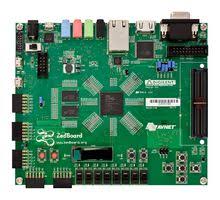
ZedBoard™ is a low-cost development board for the Xilinx Zynq ® -7000 All Programmable SoC. This board contains everything necessary to create a Linux, Android, Windows ® or other OS/RTOS-based design. Additionally, several expansion connectors expose the processing system and programmable logic I/Os for easy user access. Take advantage of the Zynq-7000 AP SoC’s tightly coupled ARM ® processing system and 7 series programmable logic to create unique and powerful designs with ZedBoard. ZedBoard is supported by the zedboard.org community website where users can collaborate with other engineers also working on Zynq designs.
Zynq-7000 ZedBoard Development Kit
^Family Name Zynq-7000
^Type Development Kit
^Family AES-Z7EV-7Z020-G
^Kit Includes Board; Power Supply ; ISE WebPACK (Devic e Locked)
^Memory Type DDR3
^Memory Size 512MB
^Configuration Memory 32MB QSPI
^USB USB OTG; USB-Serial Bridge
^Interface Standards FMC LPC; Pmod; XADC
^Display Mode HDMI Output; VGA Output; OLED Output
^Memory Card Interface SD Card
^Category Development Kits
^Manufacturer Avnet Design Services – Custom
^Zynq-7000 SoC XC7Z020-CLG484-1
^512 MB DDR3 SDRAM memory
^256 Mbit Quad-SPI serial Flash memory
^128 x 32 OLED display panel
^IS audio CODEC
^SD card socket
^On-board USB-JTAG Programming
^RJ45 socket: 10/100/1000 Ethernet
^USB OTG 2.0 and USB-UART bridge
^PS & PL I/O expansion (FMC, Pmod compatible, XADC)
^HDMI 1080p socket
^VGA socket
^Applications: Video processing, Motor control, Software acceleration, Linux/Android/RTOS development, Embedded ARM processing, General Zynq-7000 SoC prototyping
^Supplied with
^
^4GB SD Card, Micro-USB cable, USB Adapter: Male Micro-B to Female Standard-A, Getting Started Guide, ISE WebPACK with device-locked ChipScope license, US/Euro mains power supply (Requires adapter for UK use: RS 399-6134)
^Field Programmable Gate Arrays (FPGA)
^
^An FPGA is a semiconductor device consisting of a matrix of Configurable Logic Blocks (CLBs) connected through programmable interconnects. The user determines these interconnections by programming SRAM. A CLB can be simple (AND, OR gates, etc) or complex (a block of RAM). The FPGA allows changes to be made to a design even after the device is soldered into a PCB.
Datasheet:GS-AES-Z7EV-7Z020-G-V7.pdf
