Description
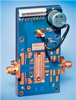
CREE CMPA801B025F-TB RF Amplifier 8.0-11.0GHz 25Watt Eval Board
Wolfspeed’s CMPA801B025F is a gallium-nitride (GaN) HEMT-based monolithic microwave integrated circuit (MMIC). GaN has superior properties compared to silicon or gallium arsenide, including higher breakdown voltage, higher saturated electron drift velocity and higher thermal conductivity. GaN HEMTs also offer greater power density and wider bandwidths compared to Si and GaAs transistors. This MMIC is available in a 10-lead metal/ceramic flanged package for optimal electrical and thermal performance.
Manufacturer: Cree, Inc.
^Product Category: RF Amplifier
^RoHS: RoHS Compliant Details
^Type: Power Amplifier
^Operating Frequency: 8.5 GHz to 11 GHz
^Gain: 16 dB
^NF – Noise Figure: –
^P1dB – Compression Point: 45.8 dBm
^OIP3 – Third Order Intercept: –
^Test Frequency: –
^Operating Supply Voltage: 28 V
^Operating Supply Current: 1.2 A
^Maximum Operating Temperature: + 130 C
^Mounting Style: Screw
^Package / Case: –
^Packaging: Bulk
^Amplifier Type: Power
^Brand: Cree, Inc.
^Development Kit: –
^Frequency Range: 8.5 GHz to 11 GHz
^Input Return Loss: – 6 dB
^Isolation dB: –
^Minimum Operating Temperature: – 40 C
^Number of Channels: 1 Channel
^Pd – Power Dissipation: 77 W
^Technology: GaN
Cree’s is a gallium nitride (GaN) High Electron Mobility Transistor (HEMT) based monolithic microwave integrated circuit (MMIC). GaN has superior properties compared to silicon or gallium arsenide, including higher breakdown voltage, higher saturated electron drift velocity and higher thermal conductivity. GaN HEMTs also offer greater power density and wider bandwidths compared to Si and GaAs transistors. This MMIC is available a 10 lead metal/ceramic flanged package for optimal electrical and thermal performance.
Note : Measured in CMPA801B025F-TB under 100 uS pulse width, 10% duty.
Features
Applications
GHz Operation· 37 W POUT typical· 16 dB Power Gain· 36 % Typical PAE
· Marine Radar· Communications· Satellite Communication Uplink
Parameter Drain-source Voltage Gate-source Voltage Power Dissipation Storage Temperature Operating Junction Temperature Maximum Forward Gate Current Soldering Temperature1 Screw Torque Thermal Resistance, Junction to Case Thermal Resistance, Junction to Case Operating Temperature
Pulse Width = 100 µs, Duty Cycle = 10%, PDISS 77 W CW, 85°C, PDISS 77 W PDISS 77 W
Note: 1 Refer to the Application Note on soldering at www.cree.com/products/wireless_appnotes.asp
Electrical Characteristics (Frequency = 8.0 GHz to 11.0 GHz unless otherwise stated; = 25°C)
Characteristics DC Characteristics Gate Threshold Gate Quiscent Voltage Saturated Drain Current2 Drain-Source Breakdown Voltage RF Characteristics3 Small Signal Gain Input Return Loss Output Return Loss S22 dB VDD 28 V, IDQ 1.2 A, PIN = -20 dBm VDD 28 V, IDQ 1.2 A VDD 28 V, IDQ A No damage at all phase angles, Output Mismatch Stress VSWR 5:1 Y VDD 28 V, IDQ 1.2 A, Pulse Width = 100 µs, Duty Cycle = 10%, PIN = 30 dBm
Notes: 1 Measured on-wafer prior to packaging. 2 Scaled from PCM data. 3 Measured in the CMPA801B025F-TB.
Cree, Inc. 4600 Silicon Drive Durham, North Carolina, USA 27703 USA Tel: +1.919.313.5300 Fax: +1.919.869.2733 www.cree.com/wireless
Characteristics RF Characteristics1,2 VDD 28 V, IDQ 1.2 A, Power Added Efficiency PAE1 Frequency = 8.5 GHz, PIN = 30 dBm VDD 28 V, IDQ 1.2 A, Power Added Efficiency PAE2 Frequency = 10.0 GHz, PIN = 30 dBm VDD 28 V, IDQ 1.2 A, Power Added Efficiency PAE3 Frequency = 11.0 GHz, PIN = 30 dBm VDD 28 V, IDQ 1.2 A, PIN = 30 dBm VDD 28 V, IDQ 1.2 A, Frequency = 8.5-11.0 GHz VDD 28 V, IDQ 1.2 A, PIN 1 W VDD 28 V, IDQ 1.2 A, PIN = 30 dBm Symbol Min. Typ. Max. Units Conditions
Power Gain Pulse Amplitude Droop Output Power Output Power
Notes: 1 Pulse Width 100 S, Duty Cycle 10 2 Measured in CMPA801B025F-TB.
Parameter Human Body Model Charge Device Model
Manufacturer Part Number: CMPA801B025F-TB
Manufacturer: Electronic Components


