69
High Voltage MLC Chips
For 600V to 5000V Application
1808
A
A
271
K
A
1
1
A
HOW TO ORDER
DIMENSIONS
millimeters (inches)
AVX
Voltage Temperature
Capacitance Code
Capacitance
Test
Termination*
Style
600V = C
Coefficient
(2 significant digits
Tolerance
Level
1 = Pd/Ag
1206
1000V = A
C0G = A
+ no. of zeros)
C0G: J = ±5%
A = Standard
T = NiGuard
1210
1500V = S
X7R = C
Examples:
K = ±10%
Nickel
1808
2000V = G
10 pF = 100
M = ±20%
Barrier
1812
2500V = W
100 pF = 101
X7R: K = ±10%
Solderable
1825
3000V = H
1,000 pF = 102
M = ±20%
Plate
2220
4000V = J
22,000 pF = 223
Z = +80%, -20%
2225
5000V = K
220,000 pF = 224
3640
1 µF = 105
SIZE
1206
1210
1808*
1812*
1825*
2220*
2225*
3640*
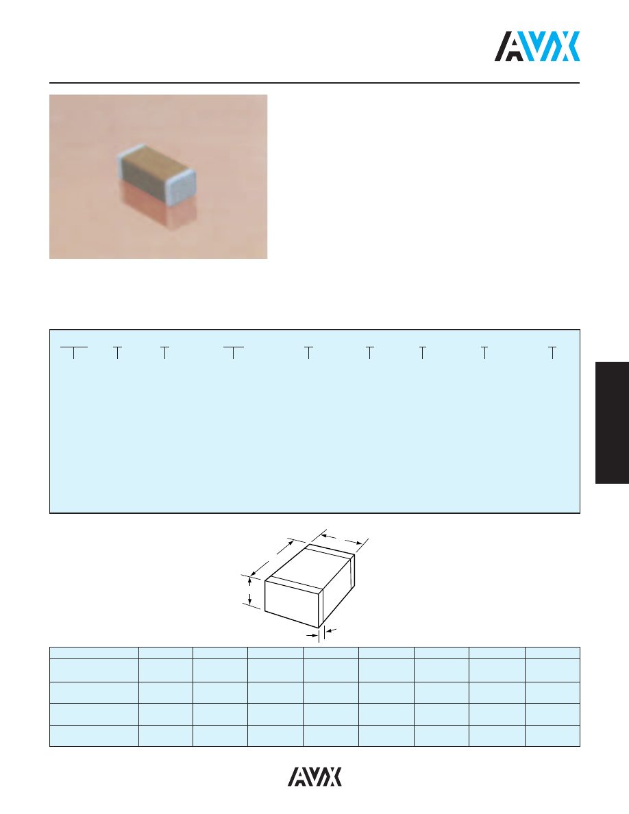
(L) Length
3.20 ± 0.2
3.20 ± 0.2
4.57 ± 0.25
4.50 ± 0.3
4.50 ± 0.3
5.7 ± 0.4
5.72 ± 0.25
9.14 ± 0.25
(0.126 ± 0.008) (0.126 ± 0.008) (0.180 ± 0.010) (0.177 ± 0.012) (0.177 ± 0.012) (0.224 ± 0.016) (0.225 ± 0.010) (0.360 ± 0.010)
(W) Width
1.60 ± 0.2
2.50 ± 0.2
2.03 ± 0.25
3.20 ± 0.2
6.40 ± 0.3
5.0 ± 0.4
6.35 ± 0.25
10.2 ± 0.25
(0.063 ± 0.008) (0.098 ± 0.008) (0.080 ± 0.010) (0.126 ± 0.008) (0.252 ± 0.012) (0.197 ± 0.016) (0.250 ± 0.010) (0.400 ± 0.010)
(T) Thickness
1.52
1.70
2.03
2.54
2.54
3.3
2.54
2.54
Max.
(0.060)
(0.067)
(0.080)
(0.100)
(0.100)
(0.130)
(0.100)
(0.100)
(t) terminal
min.
0.25 (0.010)
0.25 (0.010)
0.25 (0.010)
0.25 (0.010)
0.25 (0.010)
0.25 (0.010)
0.25 (0.010)
0.76 (0.030)
max.
0.75 (0.030)
0.75 (0.030)
1.02 (0.040)
1.02 (0.040)
1.02 (0.040)
1.02 (0.040)
1.02 (0.040)
1.52 (0.060)
High value, low leakage and small size are difficult parameters to obtain in
capacitors for high voltage systems. AVX special high voltage MLC chips
capacitors meet these performance characteristics and are designed for
applications such as snubbers in high frequency power converters,
resonators in SMPS, and high voltage coupling/DC blocking. These high
voltage chip designs exhibit low ESRs at high frequencies.
Larger physical sizes than normally encountered chips are used to make
high voltage chips. These larger sizes require that special precautions be
taken in applying these chips in surface mount assemblies. This is due
to differences in the coefficient of thermal expansion (CTE) between the
substrate materials and chip capacitors. Apply heat at less than 4°C per
second during the preheat. The preheat temperature must be within 50°C
of the peak temperature reached by the ceramic bodies through the
soldering process. Chips 1808 and larger to use reflow soldering only.
Capacitors with X7R Dielectrics are not intended for AC line filtering
applications. Contact plant for recommendations.
Capacitors may require protective surface coating to prevent external
arcing.
*Note:
Leaded terminations are available.
Styles 1825, 2225, & 3640 are available with “N”, “L” or “J” leads as seen on page 9.
“V” denotes uncoated leaded units similar to SM0 product.
“W” denotes leaded epoxy coated units similar to SM5 product.
IE 1825AA103KAV00J would be uncoated leaded part with “J” style leads.
*Reflow Soldering Only
Packaging
1 = 7" Reel
3 = 13" Reel
9 = Bulk
Special
Code
A = Standard
W
L
T
t