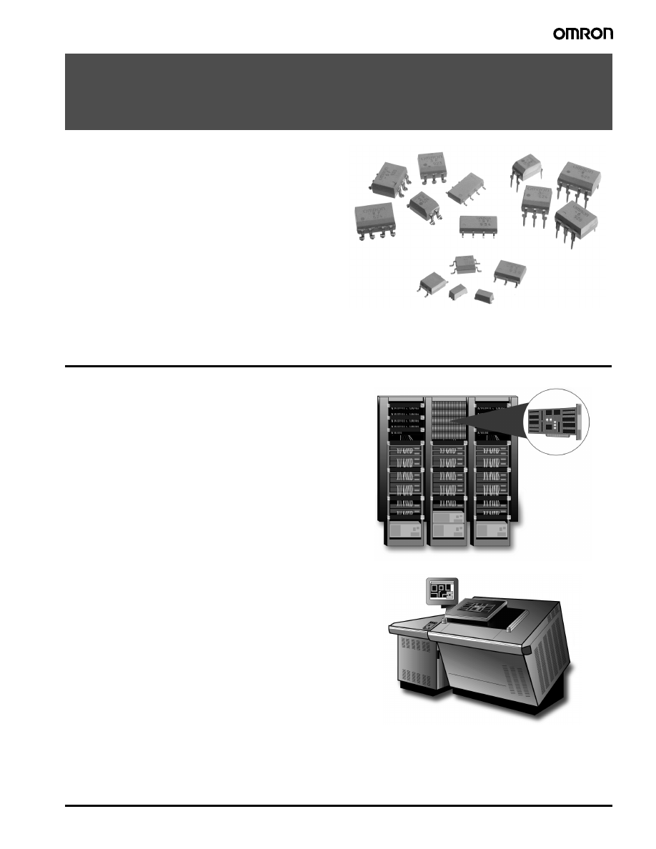
background image

MOS FET Relays


G3VM Series

23

MOS FET Relays

G3VM Series

Wide Range of Contact Forms, Sizes and 
Package Types

• Controls load voltages up to 600 V.

• Terminal packages include PCB through-hole, SMT 

gullwing, SOP, and SSOP.

• Low ON-resistance, low output capacitance, current 

limiting, and high dielectric (5000 VAC) models available.

• Packaged for efficient automatic insertion: PCB through-

hole and SMT are in tubes; tape-and-reel packaging is 
standard for SOP and SSOP models, and optional for SMT 
models (“TR” suffix).

• Complete specifications follow, divided by Package Type, 

Terminals and Contact Form.

Typical Applications

Communications

Local area network equipment

Central office circuit boards for subscriber line interfaces, 
multiplexers and other routing equipment

Wireless communications for cell phones and pagers

Set-top TV boxes with internal modems

Fax machines

PCMCIA card

Internal modems for PDA equipment and laptop computers

Test & Measurement

Board testers

IC testers

Portable voltage testers

Security

Alarm control boards

Home security systems

Garage door openers

G3VM-61ER-html.html
background image

24

MOS FET Relays 

G3VM Series

Selection Guide

Load 

voltage

Contact 

form

Package/ 

Terminal

shape

No. of 

terminals

Model

Load 

current

(mA)

Voltage 

withstand

(VAC)

ON 

resistance 

(max.)

Output 

capacitance

Additional 

features

Page no.

20V

1 Form A SMT

8

G3VM-22FO

150

2,500

8 pF (typ.)

Low ON 
resistance

62

SOP

4

G3VM-21GR

160

1,500

2.5 pF (max.)

Low pF•

70

G3VM-21GR1

300

1,500

1.5 

12 pF (max.)

Low pF•

70

SSOP

4

G3VM-21LR

150

1,500

12 pF (max.)

88

G3VM-21LR1

300

1,500

1.5 

12 pF (max.)

Low pF•

88

40V

1 Form A SOP

4

G3VM-41GR3

80

1,500

37 

1.4 pF (max.)

72

G3VM-41GR4

250

1,500

7 pF (max.)

Low pF•

74

G3VM-41GR5

300

1,500

1.5 

14 pF (max.)

Low pF•

74

G3VM-41GR6

120

1,500

15 

2 pF (max.)

Low pF•

74

SSOP

4

G3VM-41LR3

80 1,500

35 

1.4 pF (max.)

88

G3VM-41LR4

250

1,500

7 pF (max.)

Low pF•

90

G3VM-41LR5

300

1,500

1.5 

14 pF (max.)

Low pF•

90

G3VM-41LR6

120

1,500

15 

2 pF (max.)

Low pF•

90

60V

1 Form A Thru-hole

4

G3VM-61A

500

2,500

140 pF (max.)

Low ON 
resistance

32

G3VM-61A1

500

2,500

130 pF (typ.)

Low ON 
resistance

34

6

G3VM-61B

500

2,500

140 pF (max.)

Low ON 
resistance

38

G3VM-61B1

500

2,500

130 pF (typ.)

Low ON 
resistance

40

G3VM-V

300

2,500

170 pF (typ.)

Low ON 
resistance

40

8

G3VM-61CP

500

2,500

0.6 

500 pF (max.)

Low ON 
resistance

42

G3VM-61CR

2000

1,500

0.12 

1400 pF (max.) Low ON 

resistance

44

SMT

4

G3VM-61D

500

2,500

140 pF (max.)

Low ON 
resistance

52

G3VM-61D1

500

2,500

130 pF (typ.)

Low ON 
resistance

54

6

G3VM-61E

500

2,500

140 pF (max.)

Low ON 
resistance

58

G3VM-61E1

500

2,500

130 pF (typ.)

Low ON 
resistance

60

60 V

1 Form A SMT

6

G3VM-VF

300

2,500

170 pF (typ.)

Low ON 
resistance

60

8

G3VM-61FP

500

2,500

0.6 

500 pF (max.)

Low ON 
resistance

64

G3VM-61FR

2000

1,500

0.12 

1400 pF (max.) Low ON 

resistance

64

SOP

4

G3VM-61G1

400

1,500

130 pF (typ.)

Low ON 
resistance

76

G3VM-S1

400

1,500

140 pF (max.)

Low ON 
resistance

76

6

G3VM-61H1

400

1,500

130 pF (typ.)

Low ON 
resistance

80

2 Form A Thru-hole

8

G3VM-62C1

500

2,500

130 pF (typ.)

Low ON 
resistance

46

SMT

8

G3VM-62F1

500

2,500

130 pF (typ.)

Low ON 
resistance

66

SOP

8

G3VM-62J1

400

1,500

130 pF (typ.)

Low ON 
resistance

84

G3VM-SY

300

1,500

140 pF (max.)

Low ON 
resistance

86

80 V

1 Form A SOP

4

G3VM-81G1

350

1,500

1.2 

40 pF (max.)

Low ON 
resistance

76

6

G3VM-81HR

1250

1,500

0.15 

1000 pF (max.) Low ON 

resistance

80

200 V

1 Form A SOP

4

G3VM-S5

150

1,500

100 pF (typ.)

78

G3VM-61ER-html.html
background image

MOS FET Relays


G3VM Series

25


350 V

1 Form A Thru-hole

4

G3VM-2

120

2,500

35 

75 pF (typ.)

30

G3VM-2L

120

2,500

35 

75 pF (typ.)

Current 
limiting

30

G3VM-351A

120

2,500

35 

30 pF (typ.)

30

6

G3VM-351B

120

2,500

35 

30 pF (typ)

34

G3VM-3

120

2,500

35 

75 pF (typ)

36

G3VM-3L

120

2,500

35 

75 pF (typ.)

Current 
limiting

36

350 V

1 Form A SMT

4

G3VM-2F

120

2,500

35 

75 pF (typ.)

50

G3VM-2FL

120

2,500

35 

75 pF (typ.)

Current 
limiting

50

G3VM-351D

120

2,500

35 

30 pF (typ.)

50

6

G3VM-351E

120

2,500

35 

30 pF (typ.)

54

G3VM-3F

120

2,500

35 

75 pF (typ.)

56

G3VM-3FL

120

2,500

35 

75 pF (typ.)

Current 
limiting

56

SOP

4

G3VM-351G

110

1,500

35 

30 pF (typ.)

70

G3VM-S2

120

1,500

35 

75 pF (typ.)

78

6

G3VM-351H

110

1,500

35 

30 pF (typ.)

78

G3VM-S3

120

1,500

35 

75 pF (typ.)

82

1 Form A

+

1 Form B

Thru-hole

8

G3VM-355CR

120

2,500

25 

65 pF (typ.)

44

SMT

8

G3VM-355FR

120

2,500

25 

65 pF (typ.)

64

SOP

8

G3VM-355JR

120

2,500

25 

65 pF (typ.)

82

2 Form A Thru-hole

8

G3VM-352C

120

2,500

35 

30 pF (typ.)

44

G3VM-W

120

2,500

35 

75 pF (typ.)

46

G3VM-WL

120

2,500

35 

75 pF (typ.)

Current 
limiting

48

SMT

8

G3VM-352F

120

2,500

35 

30 pF (typ.)

66

G3VM-WF

120

2,500

35 

75 pF (typ.)

68

G3VM-WFL

120

2,500

35 

75 pF (typ.)

Current 
limiting

68

SOP

8

G3VM-352J

110

1,500

35 

30 pF (typ.)

82

G3VM-SW

120

1,500

35 

75 pF (typ.)

84

1 Form B Thru-hole

4

G3VM-353A

150

2,500

25 

100 pF (typ.)

32

6

G3VM-353B

150

2,500

25 

100 pF (typ.)

34

SMT

4

G3VM-353D

150

2,500

25 

100 pF (typ.)

52

6

G3VM-353E

150

2,500

25 

100 pF (typ.)

54

350 V

1 Form B SOP

4

G3VM-353G

120

1,500

25 

130 pF (typ.)

72

6

G3VM-353H

120

1,500

25 

65 pF (typ.)

80

2 Form B Thru-hole

8

G3VM-354C

120

2,500

35 

100 pF (typ.)

48

SMT

8

G3VM-354F

120

2,500

35 

100 pF (typ.)

68

SOP

8

G3VM-354J

120

1,500

25 

65 pF (typ.)

86

400 V
 

1 Form A
 

Thru-hole

4

G3VM-401A

120

2,500

35 

70 pF (typ.)

32

6

G3VM-401B

120

2,500

35 

75 pF (typ.)

36

G3VM-401BY

120

5,000

35 

75 pF (typ.)

High I/O 
isolation

38

SMT

4

G3VM-401D

120

2,500

35 

70 pF (typ.)

52

6

G3VM-401E

120

2,500

35 

75 pF (typ.)

56

G3VM-401EY

120

5,000

35 

75 pF (typ.)

High I/O 
isolation

58

SOP

4

G3VM-401G

120

1,500

35 

70 pF (typ.)

72

2 Form A Thru-hole

8

G3VM-402C

120

2,500

35 

70 pF (typ.)

46

SMT

8

G3VM-402F

120

2,500

35 

70 pF (typ.)

66

SOP

8

G3VM-402J

120

2,500

35 

70 pF (typ.)

84

600 V

1 Form A Thru-hole

6

G3VM-601BY

100

5,000

45 

100 pF (typ.)

High I/O 
isolation

38

SMT

6

G3VM-601EY

100

5,000

35 

100 pF (typ.)

High I/O 
isolation

58

Load 

voltage

Contact 

form

Package/ 

Terminal

shape

No. of 

terminals

Model

Load 

current

(mA)

Voltage 

withstand

(VAC)

ON 

resistance 

(max.)

Output 

capacitance

Additional 

features

Page no.

G3VM-61ER-html.html
background image

26

MOS FET Relays 

G3VM Series

Part Number Index and Ordering Information

Note:

“G3VM” is not printed on the actual product.

The following tables show standard quantities of G3VM relays as shipped in tubes or tape-and-reel packaging. Dimensions for tape-and-reel parts
are shown in individual data sheets that follow.

Description

Packaging

Standard pack 

quantity

Model

Page 

no.

MOSFET THRU-HOLE RELAY

Tube

50

G3VM-2

30

MOSFET SMT RELAY

Tube

50

G3VM-2F

50

MOSFET SMT RELAY

Tape-and-reel

1500

G3VM-2F(TR)

50

MOSFET SMT RELAY

Tube

50

G3VM-2FL

50

MOSFET SMT RELAY

Tape-and-reel

1500

G3VM-2FL(TR)

50

MOSFET THRU-HOLE RELAY

Tube

50

G3VM-2L

30

MOSFET SOP RELAY

Tube

50

G3VM-21GR

70

MOSFET SOP RELAY

Tape-and-reel

2500

G3VM-21GR(TR)

70

MOSFET SOP RELAY

Tube

50

G3VM-21GR1

70

MOSFET SOP RELAY

Tape-and-reel

2500

G3VM-21GR1(TR)

70

MOSFET SSOP RELAY

Tape-and-reel

1500

G3VM-21LR

88

MOSFET SSOP RELAY

Tape-and-reel

1500

G3VM-21LR1

88

MOSFET SMT RELAY

Tube

50

G3VM-22FO

62

MOSFET SMT RELAY

Tape-and-reel

1500

G3VM-22FO(TR)

62

MOSFET THRU-HOLE RELAY

Tube

50

G3VM-3

36

MOSFET SMT RELAY

Tube

50

G3VM-3F

56

MOSFET SMT RELAY

Tape-and-reel

1500

G3VM-3F(TR)

56

MOSFET SMT RELAY

Tube

50

G3VM-3FL

56

MOSFET SMT RELAY

Tape-and-reel

1500

G3VM-3FL(TR)

56

MSOFET THRU-HOLE RELAY

Tube

50

G3VM-3L

36

MOSFET THRU-HOLE RELAY

Tube

50

G3VM-351A

30

MOSFET THRU-HOLE RELAY

Tube

50

G3VM-351B

34

MOSFET SMT RELAY

Tube

50

G3VM-351D

50

MOSFET SMT RELAY

Tape-and-reel

1500

G3VM-351D(TR)

50

MOSFET SMT RELAY

Tube

50

G3VM-351E

54

MOSFET SMT RELAY

Tape-and-reel

1500

G3VM-351E(TR)

54

MOSFET SOP RELAY

Tube

50

G3VM-351G

70

MOSFET SOP RELAY

Tape-and-reel

2500

G3VM-351G(TR)

70

MOSFET SOP RELAY

Tube

50

G3VM-351H

78

MOSFETSOP RELAY

Tape-and-reel

2500

G3VM-351H(TR)

78

MOSFET THRU-HOLE RELAY

Tube

50

G3VM-352C

44

MOSFET SMT RELAY

Tube

50

G3VM-352F

66

MOSFET SMT RELAY

Tape-and-reel

1500

G3VM-352F(TR)

66

MOSFET SOP RELAY

Tube

50

G3VM-352J

82

MOSFET SOP RELAY

Tape-and-reel

2500

G3VM-352J(TR)

82

Lot No.

Model name

G3VM-61ER-html.html
background image

MOS FET Relays


G3VM Series

27

MOSFET THRU-HOLE RELAY

Tube

50

G3VM-353A

32

MOSFET THRU-HOLE RELAY

Tube

50

G3VM-353B

34

MOSFET SMT RELAY

Tube

50

G3VM-353D

52

MOSFET SMT RELAY

Tape-and-reel

1500

G3VM-353D(TR)

52

MOSFET SMT RELAY

Tube

50

G3VM-353E

54

MOSFET SMT RELAY

Tape-and-reel

1500

G3VM-353E(TR)

54

MOSFET SOP RELAY

Tube

50

G3VM-353G

72

MOSFET SOP RELAY

Tape-and-reel

2500

G3VM-353G(TR)

72

MOSFET SOP RELAY

Tube

50

G3VM-353H

80

MOSFET SOP RELAY

Tape-and-reel

2500

G3VM-353H(TR)

80

MOSFET THRU-HOLE RELAY

Tube

50

G3VM-354C

48

MOSFET SMT RELAY

Tube

50

G3VM-354F

68

MOSFET SMT RELAY

Tape-and reel

1500

G3VM-354F(TR)

68

MOSFET SOP RELAY

Tube

50

G3VM-354J

86

MOSFET SOP RELAY

Tape-and-reel

2500

G3VM-354J(TR)

86

MOSFET THRU-HOLE RELAY

Tube

50

G3VM-355CR

44

MOSFET SMT RELAY

Tube

50

G3VM-355FR

64

MOSFET SMT RELAY

Tape-and-reel

1500

G3VM-355FR(TR)

64

MOSFET SOP RELAY

Tube

50

G3VM-355JR

82

MOSFET SOP RELAY

Tape-and-reel

2500

G3VM-355JR(TR)

82

MOSFET SOP RELAY

Tube

50

G3VM-41GR3

72

MOSFET SOP RELAY

Tape-and-reel

2500

G3VM-41GR3(TR)

72

MOSFET SOP RELAY

Tube

50

G3VM-41GR4

74

MOSFET SOP RELAY

Tape-and-reel

2500

G3VM-41GR4(TR)

74

MOSFET SOP RELAY

Tube

50

G3VM-41GR5

74

MOSFET SOP RELAY

Tape-and-reel

2500

G3VM-41GR5(TR)

74

MOSFET SOP RELAY

Tube

50

G3VM-41GR6

74

MOSFET SOP RELAY

Tape-and reel

2500

G3VM-41GR6(TR)

74

MOSFET SSOP RELAY

Tape-and-reel

1500

G3VM-41LR3

88

MOSFET SSOP RELAY

Tape-and-reel

1500

G3VM-41LR4

90

MOSFET SSOP RELAY

Tape-and-reel

1500

G3VM-41LR5

90

MOSFET SSOP RELAY

Tape-and-reel

1500

G3VM-41LR6

90

MOSFET THRU-HOLE RELAY

Tube

50

G3VM-401A

32

MOSFET THRU-HOLE RELAY

Tube

50

G3VM-401B

36

MOSFET THRU-HOLE RELAY

Tube

50

G3VM-401BY

38

MOSFET SMT RELAY

Tube

50

G3VM-401D

52

MOSFET SMT RELAY

Tape-and-reel

1500

G3VM-401D(TR)

52

MOSFET SMT RELAY

Tube

50

G3VM-401E

56

MOSFET SMT RELAY

Tape-and-reel

1500

G3VM-401E(TR)

56

MOSFET SMT RELAY

Tube

50

G3VM-401EY

58

MOSFET SMT RELAY

Tape-and-reel

1500

G3VM-401EY(TR)

58

Description

Packaging

Standard pack 

quantity

Model

Page 

no.

This table continues on the next page.

G3VM-61ER-html.html
background image

28

MOS FET Relays 

G3VM Series

MOSFET SOP RELAY

Tube

50

G3VM-401G

72

MOSFET SOP RELAY

Tape-and-reel

2500

G3VM-401G(TR)

72

MOSFET THRU-HOLE RELAY

Tube

50

G3VM-402C

46

MOSFET SMT RELAY

Tube

50

G3VM-402F

66

MOSFET SMT RELAY

Tape-and-reel

1500

G3VM-402F(TR)

66

MOSFET SOP RELAY

Tube

50

G3VM-402J

84

MOSFET SOP RELAY

Tape-and reel

2500

G3VM-402J(TR)

84

MOSFET THRU-HOLE RELAY

Tube

50

G3VM-61A

32

MOSFET THRU-HOLE RELAY

Tube

50

G3VM-61A1

34

MOSFET THRU-HOLE RELAY

Tube

50

G3VM-61B

38

MOSFET THRU-HOLE RELAY

Tube

50

G3VM-61B1

40

MOSFET THRU-HOLE RELAY

Tube

50

G3VM-61CP

42

MOSFET THRU-HOLE RELAY

Tube

50

G3VM-61CR

44

MOSFET SMT RELAY

Tube

50

G3VM-61D

52

MOSFET SMT RELAY

Tape-and-reel

1500

G3VM-61D(TR)

52

MOSFET SMT RELAY

Tube

50

G3VM-61D1

54

MOSFET SMT RELAY

Tape-and-reel

1500

G3VM-61D1(TR)

54

MOSFET SMT RELAY

Tube

50

G3VM-61E

58

MOSFET SMT RELAY

Tape-and-reel

1500

G3VM-61E(TR)

58

MOSFET SMT RELAY

Tube

50

G3VM-61E1

60

MOSFET SMT RELAY

Tape-and-reel

1500

G3VM-61E1(TR)

60

MOSFET SMT RELAY

Tube

50

G3VM-61FP

64

MOSFET SMT RELAY

Tape-and-reel

1500

G3VM-61FP(TR)

64

MOSFET SMT RELAY

Tube

50

G3VM-61FR

64

MOSFET SMT RELAY

Tape-and-reel

1500

G3VM-61FR(TR)

64

MOSFET SOP RELAY

Tube

50

G3VM-61G1

76

MOSFET SOP RELAY

Tape-and-reel

2500

G3VM-61G1(TR)

76

MOSFET SOP RELAY

Tube

50

G3VM-61H1

80

MOSFET SOP RELAY

Tape-and-reel

2500

G3VM-61H1(TR)

80

MOSFET THRU-HOLE RELAY

Tube

50

G3VM-62C1

46

MOSFET SMT RELAY

Tube

50

G3VM-62F1

66

MOSFET SMT RELAY

Tape-and-reel

1500

G3VM-62F1(TR)

66

MOSFET SOP RELAY

Tube

50

G3VM-62J1

84

MOSFET SOP RELAY

Tape-and-reel

2500

G3VM-62J1(TR)

84

MOSFET THRU-HOLE RELAY

Tube

50

G3VM-601BY

38

MOSFET SMT RELAY

Tube

50

G3VM-601EY

58

MOSFET SMT RELAY

Tape-and-reel

1500

G3VM-601EY(TR)

58

MOSFET SOP RELAY

Tube

50

G3VM-81G1

76

MOSFET SOP RELAY

Tape-and-reel

2500

G3VM-81G1(TR)

76

MOSFET SOP RELAY

Tube

50

G3VM-81HR

80

MOSFET SOP RELAY

Tape-and-reel

2500

G3VM-81HR(TR)

80

Description

Packaging

Standard pack 

quantity

Model

Page 

no.

G3VM-61ER-html.html
background image

MOS FET Relays


G3VM Series

29

Specifications tables begin on the following page.

MOSFET SOP RELAY

Tube

50

G3VM-S1

76

MOSFET SOP RELAY

Tape-and-reel

2500

G3VM-S1(TR)

76

MOSFET SOP RELAY

Tube

50

G3VM-S2

78

MOSFET SOP RELAY

Tape-and-reel

2500

G3VM-S2(TR)

78

MOSFET SOP RELAY

Tube

50

G3VM-S3

82

MOSFET SOP RELAY

Tape-and-reel

2500

G3VM-S3(TR)

82

MOSFET SOP RELAY

Tube

50

G3VM-S5

78

MOSFET SOP RELAY

Tape-and-reel

2500

G3VM-S5(TR)

78

MOSFET SOP RELAY

Tube

50

G3VM-SW

84

MOSFET SOP RELAY

Tape-and-reel

2500

G3VM-SW(TR)

84

MOSFET SOP RELAY

Tube

50

G3VM-SY

86

MOSFET SOP RELAY

Tape-and-reel

2500

G3VM-SY(TR)

86

MOSFET THRU-HOLE RELAY

Tube

50

G3VM-V

40

MOSFET SMT RELAY

Tube

50

G3VM-VF

60

MOSFET SMT RELAY

Tape-and-reel

1500

G3VM-VF(TR)

60

MOSFET THRU-HOLE RELAY

Tube

50

G3VM-W

46

MOSFET SMT RELAY

Tube

50

G3VM-WF

68

MOSFET SMT RELAY

Tape-and-reel

1500

G3VM-WF(TR)

68

MOSFET SMT RELAY

Tube

50

G3VM-WFL

68

MOSFET SMT RELAY

Tape-and-reel

1500

G3VM-WFL(TR)

68

MOSFET THRU-HOLE RELAY

Tube

50

G3VM-WL

48

Description

Packaging

Standard pack 

quantity

Model

Page 

no.

G3VM-61ER-html.html
background image

30

MOS FET Relays 

G3VM Series

Specifications

G3VM-2, -2L, -351A

Maximum Rating

Electrical Characteristics

Parameter

Comments and conditions

G3VM-2

G3VM-2L

G3VM-351A

Contact form/no. of terminals

1 Form A/4 pins

1 Form A/4 pins

1 Form A/4 pins

Input (LED)

LED forward current

I

F

Typical

50 mA

50 mA

50 mA

I

FP

 (100 

µ

s pulse, 

100 pps)

Max.

1 A

1 A

1 A

Forward current 
derating

Ta 

 25

°

C

-0.5 mA/

°

C

-0.5 mA/

°

C

-0.5 mA/

°

C

Reverse voltage

V

R


Max.

5 V

6 V

5 V

Junction temperature (T

J

)

125

°

C

125

°

C

125

°

C

Output (Detector) Output voltage 

strength

V

OFF

350 V

350 V
(AC or DC peak)

350 V

Continuous load 
current

I

O

120 mA

120 mA

120 mA

ON-state current 
derating

Ta 

 25

°

C

-1.2 mA/

°

C

-1.2 mA/

°

C

-1.2 mA/

°

C

Junction temperature (T

J

)

125

°

C

125

°

C

125

°

C

Dielectric strength

V

I/O

 for 1 minute min.

2500 VAC

2500 VAC 

2500 VAC

Temperature

Ambient

Ta with no icing

-20

°

 to +85

°

C

-40

°

 to +85

°

C

-40

°

 to +85

°

C

Storage

Tstg with no icing

-55

°

 to +100

°

C

-55

°

 to +125

°

C

-55

°

 to +125

°

C

Parameter

Comments and conditions

G3VM-2

G3VM-2L

G3VM-351A

Input

LED forward voltage 
(V

F

)

I

F

=10 mA

Min.

1.0 V

1.0 V

1.0 V

Typical

1.15 V

1.15 V

1.15 V

Max.

1.3 V

1.3 V

1.3 V

Reverse current

I

Max.

10 

µ

A

10 

µ

A

10 

µ

A

Reverse voltage

V

R


Max.

5 V

6 V

5 V

Capacitance (C

T

)

V  =  0; 
freq. = 1 MHz

Typical

30 pF

30 pF

30 pF

Keep ON LED current 
(I

FT

)

I

O

 = 120 mA

Typical

2 mA

1 mA

1 mA

Max.

3 mA

3 mA

3 mA

Output

ON-resistance (R

ON

)

I

ON

=120 mA

I

F

=5 mA

Typical

22 

22 

35 

 (25 

, t< 1s)

Max.

35 

35 

50 

 (35 

, t< 1s)

OFF-state leakage 
current (I

LEAK

)

V

OFF

 = 350 V

Max.

1.0 

µ

A

1.0 

µ

A

1.0 

µ

A

Limit current (I

LIM

)

I

F

 = 5 mA, V

DD

 = 5 V, 

t = 5 ms

Min.

150 mA

Max.

300 mA

Transfer 
characteristics

I/O capacitance

(C

I/O

)

Typical

0.8 pF

0.8 pF

0.8 pF

I/O resistance

(R

IO

)

Min.

1000 M

1000 M

1000 M

Operate time 

(t

ON

)

Max.

1.0 ms

1.0 ms

1.0 ms

Release time 

(t

OFF

)

Max.

1.0 ms

1.0 ms

1.0 ms

G3VM-61ER-html.html
background image

MOS FET Relays


G3VM Series

31

Optimum Operating Conditions

Dimensions

Connections

G3VM-2, 2L

G3VM-2, 2L, 351A

Timing Chart

Parameter

Comments and conditions

G3VM-2

G3VM-2L

G3VM-351A

Output voltage strength

V

DD

Max.

280 V

280 V

280 V

Operate LED forward current

I

F

Min.

5 mA

5 mA

5 mA

Typical

7.5 mA

7.5 mA

7.5 mA

Max.

25 mA

25 mA

25 mA

Continuous load current

I

Max.

100 mA

100 mA

100 mA

Ambient temperature

T

A

 -20

°

 to 65

°

C

-20

°

 to 65

°

C

-20

°

 to 65

°

C

Item

G3VM-2

G3VM-2L

G3VM-351A

Dimensions

See page 92

See page 92

See page 92

G3VM-61ER-html.html
background image

32

MOS FET Relays 

G3VM Series

G3VM-353A, -401A, -61A

Maximum Rating

Electrical Characteristics

Optimum Operating Conditions

Parameter

Comments and conditions

G3VM-353A

G3VM-401A

G3VM-61A

Contact form/no. of terminals

1 Form B/4 pins

1 Form A/4 pins

1 Form A/4 pins

Input (LED)

LED forward current

I

F

Typical

50 mA

50 mA

50 mA

I

FP

 (100 

µ

s pulse, 

100 pps)

Max.

1 A

1 A

1 A

Forward current 
derating

Ta 

 25

°

C

-0.5 mA/

°

C

-0.5 mA/

°

C

-0.5 mA/

°

C

Reverse voltage

V

R


Max.

5 V

5 V

5 V

Junction temperature (T

J

)

125

°

C

125

°

C

125

°

C

Output (Detector) Output voltage 

strength

V

OFF

350 V

400 V

60 V

Continuous load 
current

I

O

150 mA

120 mA

500 mA

ON-state current 
derating

Ta 

 25

°

C

-1.5 mA/

°

C

-1.2 mA/

°

C

-5.0 mA/

°

C

Junction temperature (T

J

)

125

°

C

125

°

C

125

°

C

Dielectric strength

V

I/O

 for 1 minute min.

2500 VAC

2500 VAC 

2500 VAC

Temperature

Ambient

Ta with no icing

-40

°

 to +85

°

C

-40

°

 to +85

°

C

-40

°

 to +85

°

C

Storage

Tstg with no icing

-55

°

 to +125

°

C

-55

°

 to +125

°

C

-55

°

 to +125

°

C

Parameter

Comments and conditions

G3VM-353A

G3VM-401A

G3VM-61A

Input

LED forward voltage 
(V

F

)

I

F

=10 mA

Min.

1.0 V

1.0 V

1.0 V

Typical

1.15 V

1.15 V

1.15 V

Max.

1.3 V

1.3 V

1.3 V

Reverse current

I

Max.

10 

µ

A

10 

µ

A

10 

µ

A

Reverse voltage

V

R


Max.

5 V

5 V

5 V

Capacitance (C

T

)

V  =  0; 
freq. = 1 MHz

Typical

30 pF

30 pF

30 pF

Keep ON LED current 
(I

FT

)

I

O

 = 120 mA

Typical

1 mA

1 mA

1 mA

Max.

3 mA

3 mA

3 mA

Output

ON-resistance (R

ON

)

I

ON

=150 mA

I

F

=5 mA

Typical

15 

18 

 (I

ON

=500 mA)

Max.

25 

35 

 (I

ON

=500 mA)

OFF-state leakage 
current (I

LEAK

)

At V

OFF

Max.

1.0 

µ

A

1.0 

µ

A

1.0 

µ

A

Limit current (I

LIM

)

I

F

 = 5 mA, V

DD

 = 5 V, 

t = 5 ms

Min.

Max.

Transfer 
characteristics

I/O capacitance

(C

I/O

)

Typical

0.8 pF

0.8 pF

0.8 pF

I/O resistance

(R

IO

)

Min.

1000 M

1000 M

1000 M

Operate time 

(t

ON

)

Max.

1.0 ms

1.0 ms

1.0 ms 
(I

F

 = 10 mA)

Release time 

(t

OFF

)

Max.

3.0 ms

1.0 ms

1.0 ms
(I

F

 = 10 mA)

Parameter

Comments and conditions

G3VM-353A

G3VM-401A

G3VM-61A

Output voltage strength

V

DD

Max.

280 V

320 V

48 V

Operate LED forward current

I

F

Min.

5 mA

5 mA

5 mA

Typical

7.5 mA

7.5 mA

Max.

25 mA

25 mA

25 mA

Continuous load current

I

Max.

150 mA

100 mA

400 mA

Ambient temperature

T

A

 -20

°

 to 65

°

C

-20

°

 to 65

°

C

-20

°

 to 65

°

C

G3VM-61ER-html.html
background image

MOS FET Relays


G3VM Series

33

Dimensions

Connections

G3VM-353A

G3VM-353A, 401A, 61A

Timing Chart

Item

G3VM-353A

G3VM-401A

G3VM-61A

Dimensions

See page 92

See page 92

See page 92

G3VM-61ER-html.html
background image

34

MOS FET Relays 

G3VM Series

G3VM-61A1, -351B, -353B

Maximum Rating

Electrical Characteristics

Parameter

Comments and conditions

G3VM-61A1

G3VM-351B

G3VM-353B

Contact form/no. of terminals

1 Form A/4 pins

1 Form A/6 pins

1 Form B/6 pins

Input (LED)

LED forward current

I

F

Typical

50 mA

50 mA

50 mA

I

FP

 (100 

µ

s pulse, 

100 pps)

Max.

1 A

1 A

1 A

Forward current 
derating

Ta 

 25

°

C

-0.5 mA/

°

C

-0.5 mA/

°

C

-0.5 mA/

°

C

Reverse voltage

V

R


Max.

5 V

5 V

5 V

Junction temperature (T

J

)

125

°

C

125

°

C

125

°

C

Output (Detector) Output voltage 

strength

V

OFF

60 V

350 V

350 V

Continuous load 
current

I

O

500 mA

120 mA (for A)
120 mA (for B)
240 mA (for C)

150 mA (for A)
150 mA (for B)
300 mA (for C)

ON-state current 
derating

Ta 

 25

°

C

-5.0 mA/

°

C

-1.2 mA/

°

C (for A)

-1.5 mA/

°

C (for A)

Junction temperature (T

J

)

125

°

C

125

°

C

125

°

C

Dielectric strength

V

I/O

 for 1 minute min.

2500 VAC

2500 VAC 

2500 VAC

Temperature

Ambient

Ta with no icing

-40

°

 to +85

°

C

-40

°

 to +85

°

C

-40

°

 to +85

°

C

Storage

Tstg with no icing

-55

°

 to +125

°

C

-55

°

 to +125

°

C

-55

°

 to +125

°

C

Parameter

Comments and conditions

G3VM-61A1

G3VM-351B

G3VM-353B

Input

LED forward voltage 
(V

F

)

I

F

=10 mA

Min.

1.0 V

1.0 V

1.0 V

Typical

1.15 V

1.15 V

1.15 V

Max.

1.3 V

1.3 V

1.3 V

Reverse current

I

Max.

10 

µ

A

10 

µ

A

10 

µ

A

Reverse voltage

V

R


Max.

5 V

5 V

5 V

Capacitance (C

T

)

V  =  0; 
freq. = 1 MHz

Typical

30 pF

30 pF

30 pF

Keep ON LED current 
(I

FT

)

I

O

 = 120 mA

Typical

1.6 mA

1 mA

1 mA

Max.

3 mA

3 mA

3 mA

Output

ON-resistance (R

ON

)

I

F

=5 mA

Typical

 (I

ON

=500 mA)

35 

 (I

ON

=120 mA) for 

connection A

15 

 (I

ON

=150 mA) for 

connection A 

Max.

 (I

ON

=500 mA)

50 

 (I

ON

=120 mA) for 

connection A

25 

 (I

ON

=150 mA) for 

connection A

Typical

28 

 (I

ON

=120 mA) for 

connection B

 (I

ON

=150 mA) for 

connection B

Max.

40 

 (I

ON

=120 mA) for 

connection B

14 

 (I

ON

=150 mA) for 

connection B

Typical

14 

 (I

ON

=240 mA) for 

connection C

 (I

ON

=300 mA) for 

connection C

Max.

20 

 (I

ON

=240 mA) for 

connection C

 (I

ON

=300 mA) for 

connection C

OFF-state leakage 
current (I

LEAK

)

At V

OFF

 Max.

1.0 

µ

A

1.0 

µ

A

1.0 

µ

A

Limit current (I

LIM

)

I

F

 = 5 mA, V

DD

 = 5 V,

 t = 5 ms

Min.

Max.

Transfer 
characteristics

I/O capacitance

(C

I/O

)

Typical

0.8 pF

0.8 pF

0.8 pF

I/O resistance

(R

IO

)

Min.

1000 M

1000 M

1000 M

Operate time 

(t

ON

)

Max.

2.0 ms

1.0 ms

1.0 ms

Release time 

(t

OFF

)

Max.

0.5 ms

1.0 ms

3.0 ms

G3VM-61ER-html.html
background image

MOS FET Relays


G3VM Series

35

Optimum Operating Conditions

Dimensions

Connections

G3VM-61A1

G3VM-351B, -353B

G3VM-351B, -353B

Timing Chart

Parameter

Comments and conditions

G3VM-61A1

G3VM-351B

G3VM-353B

Output voltage strength

V

DD

Max.

48 V

280 V

280 V

Operate LED forward current

I

F

Min.

5 mA

5 mA

5 mA

Typical

7.5 mA

10 mA

Max.

25 mA

25 mA

25 mA

Continuous load current

I

Max.

500 mA

100 mA

150 mA

Ambient temperature

T

A

 -20

°

 to 65

°

C

-20

°

 to 65

°

C

-20

°

 to 65

°

C

Item

G3VM-61A1

G3VM-351B

G3VM-353B

Dimensions

See page 92

See page 92

See page 92

G3VM-61ER-html.html
background image

36

MOS FET Relays 

G3VM Series

G3VM-3, -3L, -401B

Maximum Rating

Electrical Characteristics

Parameter

Comments and conditions

G3VM-3

G3VM-3L

G3VM-401B

Contact form/no. of terminals

1 Form A/6 pins

1 Form A/6 pins

1 Form A/6 pins

Input (LED)

LED forward current

I

F

Typical

50 mA

50 mA

50 mA

I

FP

 (100 

µ

s pulse, 

100 pps)

Max.

1 A

1 A

1 A

Forward current 
derating

Ta 

 25

°

C

-0.5 mA/

°

C

-0.5 mA/

°

C

-0.5 mA/

°

C

Reverse voltage

V

R


Max.

5 V

5 V

5 V

Junction temperature (T

J

)

125

°

C

125

°

C

125

°

C

Output (Detector) Output voltage 

strength

V

OFF

60 V

350 V

400 V

Continuous load 
current

I

O

120 mA (for A)
120 mA (for B)
160 mA (for C)

120 mA 

120 mA (for A)
120 mA (for B) 
240 mA (for C)

ON-state current 
derating

Ta 

 25

°

C

-1.2 mA/

°

C (for A)

-1.2 mA/

°

C

-1.2 mA/

°

C (for A)

Junction temperature (T

J

)

125

°

C

125

°

C

125

°

C

Dielectric strength

V

I/O

 for 1 minute min.

2500 VAC

2500 VAC 

2500 VAC

Temperature

Ambient

Ta with no icing

-20

°

 to +85

°

C

-40

°

 to +85

°

C

-40

°

 to +85

°

C

Storage

Tstg with no icing

-55

°

 to +100

°

C

-55

°

 to +125

°

C

-55

°

 to +125

°

C

Parameter

Comments and conditions

G3VM-3

G3VM-3L

G3VM-401B

Input

LED forward voltage 
(V

F

)

I

F

=10 mA

Min.

1.0 V

1.0 V

1.0 V

Typical

1.15 V

1.15 V

1.15 V

Max.

1.3 V

1.3 V

1.3 V

Reverse current

I

Max.

10 

µ

A

10 

µ

A

10 

µ

A

Reverse voltage

V

R


Max.

5 V

5 V

5 V

Capacitance (C

T

)

V  =  0; 
freq. = 1 MHz

Typical

30 pF

30 pF

30 pF

Keep ON LED current 
(I

FT

)

At I

O

Typical

1 mA

Max.

3 mA

3 mA

3 mA

Output

ON-resistance (R

ON

)

I

F

=5 mA

Typical

22 

 (I

ON

=120 mA) 

for connection A

22 

 (I

ON

=120 mA) 

17 

 (I

ON

=120 mA) for 

connection A 

Max.

35 

 (I

ON

=120 mA) 

for connection A

35 

 (I

ON

=120 mA) 

35 

 (I

ON

=120 mA) for 

connection A

Typical

16 

 (I

ON

=120 mA) 

for connection B

11 

 (I

ON

=120 mA) for 

connection B

Max.

23 

 (I

ON

=120 mA) 

for connection B

20 

 (I

ON

=120 mA) for 

connection B

Typical

 (I

ON

=160 mA) 

for connection C

 (I

ON

=240 mA) for 

connection C

Max.

12 

 (I

ON

=160 mA) 

for connection C

10 

 (I

ON

=240 mA) for 

connection C

OFF-state leakage 
current (I

LEAK

)

At V

OFF

 Max.

1.0 

µ

A

1.0 

µ

A

1.0 

µ

A

Limit current (I

LIM

)

I

F

 = 5 mA, V

DD

 = 5 V,

 t = 5 ms

Min.

150 mA

Max.

300 mA

Transfer 
characteristics

I/O capacitance

(C

I/O

)

Typical

0.8 pF

0.8 pF

0.8 pF

I/O resistance

(R

IO

)

Min.

1000 M

1000 M

1000 M

Operate time 

(t

ON

)

Max.

1.0 ms

1.0 ms

1.0 ms

Release time 

(t

OFF

)

Max.

1.0 ms

1.0 ms

1.0 ms

G3VM-61ER-html.html
background image

MOS FET Relays


G3VM Series

37

Optimum Operating Conditions

Dimensions

Connections

G3VM-3L

G3VM-3, -3L, -401B

G3VM-3, -401B

Timing Chart

Parameter

Comments and conditions

G3VM-3

G3VM-3L

G3VM-401B

Output voltage strength

V

DD

Max.

280 V

280 V

320 V

Operate LED forward current

I

F

Min.

5 mA

5 mA

5 mA

Typical

7.5 mA

10 mA

7.5 mA

Max.

25 mA

25 mA

25 mA

Continuous load current

I

Max.

120 mA

120 mA

120 mA

Ambient temperature

T

A

 -20

°

 to 65

°

C

-20

°

 to 65

°

C

-20

°

 to 65

°

C

Item

G3VM-3

G3VM-3L

G3VM-401B

Dimensions

See page 92

See page 92

See page 92

G3VM-61ER-html.html
background image

38

MOS FET Relays 

G3VM Series

G3VM-401BY, -601BY, -61B

Maximum Rating

Electrical Characteristics

Parameter

Comments and conditions

G3VM-401BY

G3VM-601BY

G3VM-61B

Contact form/no. of terminals

1 Form A/6 pins

1 Form A/6 pins

1 Form A/6 pins

Input (LED)

LED forward current

I

F

Typical

50 mA

50 mA

50 mA

I

FP

 (100 

µ

s pulse, 

100 pps)

Max.

1 A

1 A

1 A

Forward current 
derating

Ta 

 25

°

C

-0.5 mA/

°

C

-0.5 mA/

°

C

-0.5 mA/

°

C

Reverse voltage

V

R


Max.

5 V

5 V

5 V

Junction temperature (T

J

)

125

°

C

125

°

C

125

°

C

Output (Detector) Output voltage 

strength

V

OFF

400 V

600 V

60 V

Continuous load 
current

I

O

120 mA (for A)
120 mA (for B) 
240 mA (for C)

100 mA (for A)
100 mA (for B) 
200 mA (for C)

500 mA (for A) 
500 mA (for B) 
1000 mA (for C)

ON-state current 
derating

Ta 

 25

°

C

-1.2 mA/

°

C (for A)

-1.0 mA/

°

C (for A)

-5.0 mA/

°

C (for A)

Junction temperature (T

J

)

125

°

C

125

°

C

125

°

C

Dielectric strength

V

I/O

 for 1 minute min.

5000 VAC

5000 VAC 

2500 VAC

Temperature

Ambient

Ta with no icing

-40

°

 to +85

°

C

-40

°

 to +85

°

C

-40

°

 to +85

°

C

Storage

Tstg with no icing

-55

°

 to +125

°

C

-55

°

 to +125

°

C

-55

°

 to +125

°

C

Parameter

Comments and conditions

G3VM-401BY

G3VM-601BY

G3VM-61B

Input

LED forward voltage 
(V

F

)

I

F

=10 mA

Min.

1.0 V

1.0 V

1.0 V

Typical

1.15 V

1.15 V

1.15 V

Max.

1.3 V

1.3 V

1.3 V

Reverse current

I

Max.

10 

µ

A

10 

µ

A

10 

µ

A

Reverse voltage

V

R


Max.

5 V

5 V

5 V

Capacitance (C

T

)

V  =  0; 
freq. = 1 MHz

Typical

30 pF

30 pF

30 pF

Keep ON LED current 
(I

FT

)

At I

O

Typical

Max.

3 mA

5 mA

3 mA

Output

ON-resistance (R

ON

)

I

F

=5 mA

Typical

17 

 (I

ON

=120 mA) 

for connection A

30 

 (I

ON

=100 mA) for 

connection A

 (I

ON

=500 mA) for 

connection A 

Max.

35 

 (I

ON

=120 mA) 

for connection A

45 

 (I

ON

=100 mA) for 

connection A

 (I

ON

=500 mA) for 

connection A

Typical

11 

 (I

ON

=120 mA) 

for connection B

23 

 (I

ON

=100 mA) for 

connection B

0.5 

 (I

ON

=500 mA) for 

connection B

Max.

20 

 (I

ON

=120 mA) 

for connection B

35 

 (I

ON

=100 mA) for 

connection B

 (I

ON

=500 mA) for 

connection B

Typical

 (I

ON

=240 mA) 

for connection C

12 

 (I

ON

=200 mA) for 

connection C

0.3 

 (I

ON

=1000 mA) 

for connection C

Max.

10 

 (I

ON

=240 mA) 

for connection C

18 

 (I

ON

=200 mA) for 

connection C

OFF-state leakage 
current (I

LEAK

)

At V

OFF

 Max.

1.0 

µ

A

1.0 

µ

A

1.0 

µ

A

Limit current (I

LIM

)

I

F

 = 5 mA, V

DD

 = 5 V,

 t = 5 ms

Min.

Max.

Transfer 
characteristics

I/O capacitance

(C

I/O

)

Typical

0.8 pF

0.8 pF

0.8 pF

I/O resistance

(R

IO

)

Min.

1000 M

1000 M

1000 M

Operate time 

(t

ON

)

Max.

1.0 ms

1.5 ms

1.0 ms

Release time 

(t

OFF

)

Max.

1.0 ms

1.0 ms

1.0 ms

G3VM-61ER-html.html
background image

MOS FET Relays


G3VM Series

39

Optimum Operating Conditions

Dimensions

Connections

G3VM-401BY, -601BY, -61B

G3VM-401BY, -601BY, -61B

Timing Chart

Parameter

Comments and conditions

G3VM-401BY

G3VM-601BY

G3VM-61B

Output voltage strength

V

DD

Max.

320 V

480 V

48 V

Operate LED forward current

I

F

Min.

5 mA

7.5 mA

5 mA

Typical

7.5 mA

15 mA

7.5 mA

Max.

25 mA

25 mA

25 mA

Continuous load current

I

Max.

120 mA

100 mA

400 mA

Ambient temperature

T

A

 -20

°

 to 65

°

C

-20

°

 to 65

°

C

-20

°

 to 65

°

C

Item

G3VM-401BY

G3VM-601BY

G3VM-61B

Dimensions

See page 92

See page 92

See page 92

G3VM-61ER-html.html
background image

40

MOS FET Relays 

G3VM Series

G3VM-61B1, -V

Maximum Rating

Electrical Characteristics

Parameter

Comments and conditions

G3VM-61B1

G3VM-V

Contact form/no. of terminals

1 Form A/6 pins

1 Form A/6 pins

Input (LED)

LED forward current

I

F

Typical

50 mA

50 mA

I

FP

 (100 

µ

s pulse, 100 

pps)

Max.

1 A

1 A

Forward current derating

Ta 

 25

°

C

-0.5 mA/

°

C

-0.5 mA/

°

C

Reverse voltage

V

R


Max.

5 V

5 V

Junction temperature (T

J

)

125

°

C

125

°

C

Output (Detector)

Output voltage strength

V

OFF

60 V

60 V

Continuous load current

I

O

500 mA (for A)
500 mA (for B)
1000 mA (for C)

300 mA (for A)
450 mA (for B)
600 mA (for C)

ON-state current derating

Ta 

 25

°

C

-5.0 mA/

°

C (for A)

-3.0 mA/

°

C (for A)

Junction temperature (T

J

)

125

°

C

125

°

C

Dielectric strength

V

I/O

 for 1 minute min.

2500 VAC

2500 VAC 

Temperature

Ambient

Ta with no icing

-40

°

 to +85

°

C

-20

°

 to +85

°

C

Storage

Tstg with no icing

-55

°

 to +125

°

C

-55

°

 to +100

°

C

Parameter

Comments and conditions

G3VM-61B1

G3VM-V

Input

LED forward voltage (V

F

)

I

F

=10 mA

Min.

1.0 V

1.0 V

Typical

1.15 V

1.15 V

Max.

1.3 V

1.3 V

Reverse current

I

Max.

10 

µ

A

10 

µ

A

Reverse voltage

V

R

 Max.

V

V

Capacitance (C

T

)

V  =  0; 
freq. = 1 MHz

Typical

30 pF

30 pF

Keep ON LED current (I

FT

) At  I

O

Typical

1.6 mA

1 mA

Max.

3 mA

5 mA

Output

ON-resistance (R

ON

)

I

F

=5 mA

Typical

 (I

ON

=500 mA) for 

connection A

1.4 

 (I

ON

=300 mA) for 

connection A

Max.

 (I

ON

=500 mA) for 

connection A

 (I

ON

=300 mA) for 

connection A

Typical

0.5 

 (I

ON

=500 mA) for 

connection B

0.7 

 (I

ON

=450 mA) for 

connection B

Max.

 (I

ON

=500 mA) for 

connection B

 (I

ON

=450 mA) for 

connection B

Typical

0.25 

 (I

ON

=1000 mA) for 

connection C

0.35 

 (I

ON

=600 mA) for 

connection C

Max.

0.5 

 (I

ON

=600 mA) for 

connection C

OFF-state leakage current 
(I

LEAK

)

At V

OFF

 Max.

1.0 

µ

A

1.0 

µ

A

Limit current (I

LIM

)

I

F

 = 5 mA, V

DD

 = 5 V,

 t = 5 ms

Min.

Max.

Transfer 
characteristics

I/O capacitance

(C

I/O

)

Typical

0.8 pF

0.8 pF

I/O resistance

(R

IO

)

Min.

1000 M

1000 M

Operate time 

(t

ON

)

Max.

2.0 ms

1.0 ms

Release time 

(t

OFF

)

Max.

0.5 ms

1.0 ms

G3VM-61ER-html.html
background image

MOS FET Relays


G3VM Series

41

Optimum Operating Conditions

Dimensions

Connections

G3VM-61B1, -V

G3VM-61B1, -V

Timing Chart

Parameter

Comments and conditions

G3VM-61B1

G3VM-V

Output voltage strength

V

DD

Max.

48 V

48V

Operate LED forward current

I

F

Min.

5 mA

7.5 mA

Typical

7.5 mA

15 mA

Max.

25 mA

25 mA

Continuous load current

I

Max.

500 mA

300 mA

Ambient temperature

T

A

 -20

°

 to 65

°

C

-20

°

 to 80

°

C

Item

G3VM-61B1

G3VM-V

Dimensions

See page 92

See page 92

G3VM-61ER-html.html
background image

42

MOS FET Relays 

G3VM Series

G3VM-61CP

Maximum Rating

Electrical Characteristics

Parameter

Comments and conditions

G3VM-61CP

Contact form/no. of terminals

1 Form A/8 pins

Input (LED)

LED forward current

I

F

Typical

50 mA

I

FP

 (100 

µ

s pulse, 100 pps)

Max.

1 A

Forward current derating

Ta 

 25

°

C

-0.5 mA/

°

C

Reverse voltage

V

R

 Max.

V

Junction temperature (T

J

)

125

°

C

Output (Detector)

Output voltage strength

V

OFF

60 V

Continuous load current

I

O

500 mA

ON-state current derating

Ta 

 25

°

C

-5.0 mA/

°

C

Junction temperature (T

J

)

125

°

C

Dielectric strength

V

I/O

 for 1 minute min.

2500 VAC

Temperature

Ambient

Ta with no icing

-40

°

 to +85

°

C

Storage

Tstg with no icing

-55

°

 to +125

°

C

Parameter

Comments and conditions

G3VM-61CP

Input

LED forward voltage (V

F

)

I

F

=10 mA

Min.

1.0 V

Typical

1.2 V

Max.

1.4 V

Reverse current

I

Max.

15 

µ

A

Reverse voltage

V

R

 Max.

V

Capacitance (C

T

)

V  =  0; 
freq. = 1 MHz

Typical

15 pF

Keep ON LED current (I

FT

)

At  I

O

Typical

Max.

5 mA

Output

ON-resistance (R

ON

)

I

F

=5 mA

Typical

0.3 

 (I

ON

=500 mA)

Max.

0.6 

 (I

ON

=500 mA)

Typical

Max.

Typical

Max.

OFF-state leakage current (I

LEAK

) At  V

OFF

 Max.

1.0 

µ

A

Capacitance

COFF

Typical

200 pF

Max.

500 pF

Transfer characteristics

I/O capacitance

(C

I/O

)

Typical

0.8 pF

I/O resistance

(R

IO

)

Min.

1000 M

Operate time 

(t

ON

)

Max.

2.0  ms

Release time 

(t

OFF

)

Max.

0.5  ms

G3VM-61ER-html.html
background image

MOS FET Relays


G3VM Series

43

Optimum Operating Conditions

Dimensions

Connections

G3VM-61CP

Timing Chart

Parameter

Comments and conditions

G3VM-61CP

Output voltage strength

V

DD

Max.

48 V

Operate LED forward current

I

F

Min.

10 mA

Typical

— mA

Max.

30 mA

Continuous load current

I

Max.

500 mA

Ambient temperature

T

A

 -25

°

 to 50

°

C

Item

G3VM-61CP

Dimensions

See page 93

G3VM-61ER-html.html
background image

44

MOS FET Relays 

G3VM Series

G3VM-61CR, 355CR, 352C

Maximum Rating

Electrical Characteristics

Parameter

Comments and conditions

G3VM-61CR

G3VM-355CR

G3VM-352C

Contact form/no. of terminals

1 Form A/8 pins

1FormA+1FormB/ 
8 pins

2 Form A/8 pins

Input (LED)

LED forward current

I

F

Typical

50 mA

50 mA

50 mA

I

FP

 (100 

µ

s pulse, 

100 pps)

Max.

1  A

1  A

1  A

Forward current 
derating

Ta 

 25

°

C

-0.5 mA/

°

C

-0.5  mA/

°

C

-0.5  mA/

°

C

Reverse voltage

V

R


Max.

6  V

5  V

5  V

Junction temperature (T

J

)

125

°

C

125

°

C

125

°

C

Output (Detector) Output voltage 

strength

V

OFF

60 V

350 V

350 V

Continuous load 
current

I

O

2000 mA

120 mA 

120 mA

ON-state current 
derating

Ta 

 25

°

C

-20 mA/

°

C

-1.2  mA/

°

C

-1.2  mA/

°

C

Junction temperature (T

J

)

125

°

C

125

°

C

125

°

C

Dielectric strength

V

I/O

 for 1 minute min.

1500 VAC

2500 VAC 

2500 VAC

Temperature

Ambient

Ta with no icing

-20

°

 to +85

°

C

-40

°

 to +85

°

C

-40

°

 to +85

°

C

Storage

Tstg with no icing

-55

°

 to +125

°

C

-55

°

 to +125

°

C

-55

°

 to +100

°

C

Parameter

Comments and conditions

G3VM-61CR

G3VM-355CR

G3VM-352C

Input

LED forward voltage 
(V

F

)

I

F

=10 mA

Min.

1.0 V

1.0 V

1.0 V

Typical

1.2 V

1.15 V

1.15 V

Max.

1.4 V

1.3 V

1.3 V

Reverse current

I

Max.

10 

µ

A

10 

µ

A

10 

µ

A

Reverse voltage

V

R


Max.

6  V

5  V

5  V

Capacitance (C

T

)

V  =  0; 
freq. = 1 MHz

Typical

15 pF

30 pF

30 pF

Keep ON LED current 
(I

FT

)

At I

O

Typical

1 mA

1 mA

Max.

5 mA

3 mA

3 mA

Output

ON-resistance (R

ON

)

I

F

=5 mA (1a)

Typical

15 

 (I

ON

=120 mA)

35 

 (25 

, t 

 1s)

Max.

0.12 

 25 

 (I

ON

=120 mA) 

50 

 (35 

, t 

 1s)

I

F

=0 mA (1b)

Typical

15 

 (I

ON

=120 mA)

Max.

25 

 (I

ON

=120 mA) 

Typical

Max.

OFF-state leakage 
current (I

LEAK

)

At V

OFF

 Max.

4.0 

µ

A

1.0 

µ

A

1.0 

µ

A

Capacitance

COFF

Typical

— pF

Max.

—  pF

Transfer 
characteristics

I/O capacitance

(C

I/O

)

Typical

0.8 pF

0.8 pF

0.8 pF

I/O resistance

(R

IO

)

Min.

1000 M

1000 M

1000 M

Operate time 

(t

ON

)

Max.

5.0 ms

1.0 ms

1.0 ms

Release time 

(t

OFF

)

Max.

3.5 ms

3.0 ms

1.0 ms

G3VM-61ER-html.html
background image

MOS FET Relays


G3VM Series

45

Optimum Operating Conditions

Dimensions

Connections

G3VM-61CR

G3VM-352C

G3VM-355CR

Timing Chart

Parameter

Comments and conditions

G3VM-61CR

G3VM-355CR

G3VM-352C

Output voltage strength

V

DD

Max.

48 V

280V

280 V

Operate LED forward current

I

F

Min.

10 mA

5 mA

5 mA

Typical

— mA

7.5 mA

Max.

30 mA

25 mA

25 mA

Continuous load current

I

Max.

2000 mA

120 mA

100 mA

Ambient temperature

T

A

 -25

°

 to 50

°

C

-20

°

 to 65

°

C

-20

°

 to 65

°

C

Item

G3VM-61CR

G3VM-355CR

G3VM-352C

Dimensions

See page 93

See page 93

See page 93

G3VM-61ER-html.html
background image

46

MOS FET Relays 

G3VM Series

G3VM-402C, -62C1, -W

Maximum Rating

Electrical Characteristics

Parameter

Comments and conditions

G3VM-402C

G3VM-62C1

G3VM-W

Contact form/no. of terminals

2 Form A/8 pins

2 Form A/8 pins

2 Form A/8 pins

Input (LED)

LED forward current

I

F

Typical

50 mA

50 mA

50 mA

I

FP

 (100 

µ

s pulse, 

100 pps)

Max.

1  A

1  A

1  A

Forward current 
derating

Ta 

 25

°

C

-0.5 mA/

°

C

-0.5  mA/

°

C

-0.5  mA/

°

C

Reverse voltage

V

R


Max.

5  V

5  V

5  V

Junction temperature (T

J

)

125

°

C

125

°

C

125

°

C

Output (Detector) Output voltage 

strength

V

OFF

400 V

60 V

350 V

Continuous load 
current

I

O

120 mA

500 mA 

120 mA

ON-state current 
derating

Ta 

 25

°

C

-1.2 mA/

°

C

-5.0  mA/

°

C

-1.2  mA/

°

C

Junction temperature (T

J

)

125

°

C

125

°

C

125

°

C

Dielectric strength

V

I/O

 for 1 minute min.

2500 VAC

2500 VAC 

2500 VAC

Temperature

Ambient

Ta with no icing

-40

°

 to +85

°

C

-40

°

 to +85

°

C

-20

°

 to +85

°

C

Storage

Tstg with no icing

-55

°

 to +125

°

C

-55

°

 to +125

°

C

-55

°

 to +100

°

C

Parameter

Comments and conditions

G3VM-402C

G3VM-62C1

G3VM-W

Input

LED forward voltage 
(V

F

)

I

F

=10 mA

Min.

1.0 V

1.0 V

1.0 V

Typical

1.15 V

1.15 V

1.15 V

Max.

1.3 V

1.3 V

1.3 V

Reverse current

I

Max.

10 

µ

A

10 

µ

A

10 

µ

A

Reverse voltage

V

R


Max.

5 V

5 V

5 V

Capacitance (C

T

)

V  =  0;
freq. = 1 MHz

Typical

30 pF

30 pF

30 pF

Keep ON LED current 
(I

FT

)

At I

O

Typical

1

1.6 mA

2 mA

Max.

3 mA

3 mA

3 mA

Output

ON-resistance (R

ON

)

I

F

=5 mA (1a)

Typical

18 

 (I

ON

=120 mA)

1.0 

 (I

ON

=500 mA)

22 

 (I

ON

=120 mA)

Max.

35 

 (I

ON

=120 mA)

2.0 

 (I

ON

=500 mA) 

35 

 (I

ON

=120 mA)

I

F

=0 mA (1b)

Typical

Max.

Typical

Max.

OFF-state leakage 
current (I

LEAK

)

At V

OFF

 Max.

1.0 

µ

A

1.0 

µ

A

1.0 

µ

A

Capacitance

COFF

Typical

Max.

Transfer 
characteristics

I/O capacitance

(C

I/O

)

Typical

0.8 pF

0.8 pF

0.8 pF

I/O resistance

(R

IO

)

Min.

1000 M

1000 M

1000 M

Operate time 

(t

ON

)

Max.

1.0 ms

2.0 ms

1.0 ms

Release time 

(t

OFF

)

Max.

1.0 ms

0.5 ms

1.0 ms

G3VM-61ER-html.html
background image

MOS FET Relays


G3VM Series

47

Optimum Operating Conditions

Dimensions

Connections

G3VM-402C, -62C1, -W

Timing Chart

Parameter

Comments and conditions

G3VM-402C

G3VM-62C1

G3VM-W

Output voltage strength

V

DD

Max.

320 V

48 V

280 V

Operate LED forward current

I

F

Min.

5 mA

5 mA

5 mA

Typical

7.5 mA

7.5

7.5 mA

Max.

25 mA

25 mA

25 mA

Continuous load current

I

Max.

100 mA

500 mA

100 mA

Ambient temperature

T

A

 -20

°

 to 65

°

C

-20

°

 to 65

°

C

-20

°

 to 65

°

C

Item

G3VM-402C

G3VM-62C1

G3VM-W

Dimensions

See page 93

See page 93

See page 93

G3VM-61ER-html.html
background image

48

MOS FET Relays 

G3VM Series

G3VM-WL, -354C

Maximum Rating

Electrical Characteristics

Parameter

Comments and conditions

G3VM-WL

G3VM-354C

Contact form/no. of terminals

2 Form A/8 pins

2 Form B/8 pins

Input (LED)

LED forward current

I

F

Typical

50 mA

50 mA

I

FP

 (100 

µ

s pulse, 

100 pps)

Max.

1 A

1 A

Forward current 
derating

Ta 

 25

°

C

-0.5 mA/

°

C

-0.5 mA/

°

C

Reverse voltage

V

R


Max.

6 V

5 V

Junction temperature (T

J

)

125

°

C

125

°

C

Output (Detector) Output voltage 

strength

V

OFF

350 V

350 V

Continuous load 
current

I

O

120 mA

150 mA 

ON-state current 
derating

Ta 

 25

°

C

-1.2 mA/

°

C

-1.5 mA/

°

C

Junction temperature (T

J

)

125

°

C

125

°

C

Dielectric strength

V

I/O

 for 1 minute min.

2500 VAC

2500 VAC 

Temperature

Ambient

Ta with no icing

-40

°

 to +85

°

C

-40

°

 to +85

°

C

Storage

Tstg with no icing

-55

°

 to +125

°

C

-55

°

 to +125

°

C

Parameter

Comments and conditions

G3VM-WL

G3VM-354C

Input

LED forward voltage 
(V

F

)

I

F

=10 mA

Min.

1.0 V

1.0 V

Typical

1.15 V

1.15 V

Max.

1.3 V

1.3 V

Reverse current

I

Max.

10 

µ

A

10 

µ

A

Reverse voltage

V

R


Max.

6 V

5 V

Capacitance (C

T

)

V  =  0; 
freq. = 1 MHz

Typical

30 pF

30 pF

Keep ON LED current 
(I

FT

)

At I

O

Typical

1

1 mA

Max.

3 mA

3 mA

Output

ON-resistance (R

ON

)

I

F

=5 mA 

Typical

22 

 (I

ON

=120 mA) 15 

 (I

ON

=150 mA)

Max.

35 

 (I

ON

=120 mA) 25 

 (I

ON

=150 mA) 

Typical

Max.

Typical

Max.

OFF-state leakage 
current (I

LEAK

)

At V

OFF

 Max.

1.0 

µ

A

1.0 

µ

A

Limit current

I

LIM

Min.

150 mA

Max.

300 mA

Transfer 
characteristics

I/O capacitance

(C

I/O

)

Typical

0.8 pF

0.8 pF

I/O resistance

(R

IO

)

Min.

1000 M

1000 M

Operate time 

(t

ON

)

Max.

1.0 ms

1.0 ms

Release time 

(t

OFF

)

Max.

1.0 ms

3.0 ms

G3VM-61ER-html.html
background image

MOS FET Relays


G3VM Series

49

Optimum Operating Conditions

Dimensions

Connections

G3VM-WL, -354C

Timing Chart

Parameter

Comments and conditions

G3VM-WL

G3VM-354C

Output voltage strength

V

DD

Max.

280 V

280 V

Operate LED forward current

I

F

Min.

5 mA

5 mA

Typical

7.5 mA

Max.

25 mA

25 mA

Continuous load current

I

Max.

100 mA

150 mA

Ambient temperature

T

A

 -20

°

 to 65

°

C

-20

°

 to 65

°

C

Item

G3VM-WL

G3VM-354C

Dimensions

See page 93

See page 93

G3VM-61ER-html.html
background image

50

MOS FET Relays 

G3VM Series

G3VM-2F(TR), -2FL(TR), -351D(TR)

Maximum Rating

Electrical Characteristics

Parameter

Comments and conditions

G3VM-2F,
G3VM-2F(TR)

G3VM-2FL,
G3VM-2FL(TR)

G3VM-351D, 
G3VM-351D(TR)

Contact form/no. of terminals

1 Form A/4 pins

1 Form A/4 pins

1 Form A/4 pins

Input (LED)

LED forward current

I

F

Typical

50 mA

50 mA

50 mA

I

FP

 (100 

µ

s pulse, 

100 pps)

Max.

1 A

1 A

1 A

Forward current 
derating

Ta 

 25

°

C

-0.5 mA/

°

C

-0.5 mA/

°

C

-0.5 mA/

°

C

Reverse voltage

V

R


Max.

5 V

6 V

5 V

Junction temperature (T

J

)

125

°

C

125

°

C

125

°

C

Output (Detector) Output voltage 

strength

V

OFF

350 V

350 V

350 V

Continuous load 
current

I

O

120 mA

120 mA

120 mA

ON-state current 
derating

Ta 

 25

°

C

-1.2 mA/

°

C

-1.2 mA/

°

C

-1.2 mA/

°

C

Junction temperature (T

J

)

125

°

C

125

°

C

125

°

C

Dielectric strength

V

I/O

 for 1 minute min.

2500 VAC

2500 VAC 

2500 VAC

Temperature

Ambient

Ta with no icing

-20

°

 to +85

°

C

-40

°

 to +85

°

C

-40

°

 to +85

°

C

Storage

Tstg with no icing

-55

°

 to +100

°

C

-55

°

 to +125

°

C

-55

°

 to +100

°

C

Parameter

Comments and conditions

G3VM-2F,
G3VM-2F(TR)

G3VM-2FL,
G3VM-2FL(TR)

G3VM-351D, 
G3VM-351D(TR)

Input

LED forward voltage 
(V

F

)

I

F

=10 mA

Min.

1.0 V

1.0 V

1.0 V

Typical

1.15 V

1.15 V

1.15 V

Max.

1.3 V

1.3 V

1.3 V

Reverse current

I

Max.

10 

µ

A

10 

µ

A

10 

µ

A

Reverse voltage

V

R


Max.

5 V

6 V

5 V

Capacitance (C

T

)

V  =  0; 
freq. = 1 MHz

Typical

30 pF

30 pF

30 pF

Keep ON LED current 
(I

FT

)

At I

O

Typical

2 mA (I

O

 = 100 mA) 1 mA (I

O

 = 120 mA)

1 mA (I

O

 = 120 mA)

Max.

3 mA (I

O

 = 100 mA

3 mA (I

O

 = 120 mA)

3 mA (I

O

 = 120 mA)

Output

ON-resistance (R

ON

)

I

ON

=120 mA

I

F

=5 mA

Typical

22 

22 

35 

 (25 

, t< 1s)

Max.

35 

35 

50 

 (35 

, t< 1s)

OFF-state leakage 
current (I

LEAK

)

V

OFF

 = 350 V

Max.

1.0 

µ

A

1.0 

µ

A

1.0 

µ

A

Limit current (I

LIM

)

I

F

 = 5 mA, V

DD

 = 5 V, 

t = 5 ms

Min.

150 mA

Max.

300 mA

Transfer 
characteristics

I/O capacitance

(C

I/O

)

Typical

0.8 pF

0.8 pF

0.8 pF

I/O resistance

(R

IO

)

Min.

1000 M

1000 M

1000 M

Operate time 

(t

ON

)

Max.

1.0 ms

1.0 ms

1.0 ms

Release time 

(t

OFF

)

Max.

1.0 ms

1.0 ms

1.0 ms

G3VM-61ER-html.html
background image

MOS FET Relays


G3VM Series

51

Optimum Operating Conditions

Dimensions

Connections

G3VM-2F, -2F(TR), -2FL, -2FL(TR)

G3VM-2F, -2F(TR), -2FL, -2FL(TR), -351D, -351D(TR)

Timing Chart

Parameter

Comments and conditions

G3VM-2F,
G3VM-2F(TR)

G3VM-2FL,
G3VM-2FL(TR)

G3VM-351D, 
G3VM-351D(TR)

Output voltage strength

V

DD

Max.

280 V

280 V

280 V

Operate LED forward current

I

F

Min.

5 mA

5 mA

5 mA

Typical

7.5 mA

7.5 mA

7.5 mA

Max.

25 mA

25 mA

25 mA

Continuous load current

I

Max.

100 mA

100 mA

100 mA

Ambient temperature

T

A

 -20

°

 to 65

°

C

-20

°

 to 65

°

C

-20

°

 to 65

°

C

Item

G3VM-2F,
G3VM-2F(TR)

G3VM-2FL,
G3VM-2FL(TR)

G3VM-351D, 
G3VM-351D(TR)

Dimensions

See pages 94, 98

See pages 94, 98

See pages 94, 98

G3VM-61ER-html.html
background image

52

MOS FET Relays 

G3VM Series

G3VM-353D(TR), -401D(TR), -61D(TR)

Maximum Rating

Electrical Characteristics

Parameter

Comments and conditions

G3VM-353D,
G3VM-353D(TR)

G3VM-401D, 
G3VM-401D(TR)

G3VM-61D,
G3VM-61D(TR)

Contact form/no. of terminals

1 Form B/4 pins

1 Form A/4 pins

1 Form A/4 pins

Input (LED)

LED forward current

I

F

Typical

50 mA

50 mA

50 mA

I

FP

 (100 

µ

s pulse, 

100 pps)

Max.

1  A

1  A

1  A

Forward current 
derating

Ta 

 25

°

C

-0.5 mA/

°

C

-0.5 mA/

°

C

-0.5 mA/

°

C

Reverse voltage

V

R


Max.

5  V

5  V

5  V

Junction temperature (T

J

)

125

°

C

125

°

C

125

°

C

Output 
(Detector)

Output voltage 
strength

V

OFF

350 V

400 V

60 V

Continuous load 
current

I

O

150 mA

120 mA

500 mA

ON-state current 
derating

Ta 

 25

°

C

-1.5 mA/

°

C

-1.2 mA/

°

C

-5.0 mA/

°

C

Junction temperature (T

J

)

125

°

C

125

°

C

125

°

C

Dielectric strength

V

I/O

 for 1 minute min.

2500 VAC

2500 VAC 

2500 VAC

Temperature

Ambient

Ta with no icing

-40

°

 to +85

°

C

-40

°

 to +85

°

C

-40

°

 to +85

°

C

Storage

Tstg with no icing

-55

°

 to +125

°

C

-55

°

 to +100

°

C

-55

°

 to +125

°

C

Parameter

Comments and conditions

G3VM-353D,
G3VM-353D(TR)

G3VM-401D, 
G3VM-401D(TR)

G3VM-61D,
G3VM-61D(TR)

Input

LED forward voltage 
(V

F

)

I

F

=10 mA

Min.

1.0 V

1.0 V

1.0 V

Typical

1.15 V

1.15 V

1.15 V

Max.

1.3 V

1.3 V

1.3 V

Reverse current

I

Max.

10 

µ

A

10 

µ

A

10 

µ

A

Reverse voltage

V

R


Max.

5  V

5  V

5  V

Capacitance (C

T

)

V  =  0; 
freq. = 1 MHz

Typical

30 pF

30 pF

30 pF

Keep ON LED current 
(I

FT

)

At I

ON


Typical

1 mA

1 mA

1 mA

Max.

3 mA

3 mA

3 mA

Output

ON-resistance (R

ON

)

At  I

O

Typical

15 

 (I

ON

=150 mA)

18 

 (I

ON

=120 mA)

 (I

ON

=500 mA)

Max.

25 

 (I

ON

=150 mA)

35 

 (I

ON

=120 mA)

 (I

ON

=500 mA)

OFF-state leakage 
current (I

LEAK

)

At V

OFF

Max.

1.0 

µ

A

1.0 

µ

A

1.0 

µ

A

Limit current (I

LIM

)

I

F

 = 5 mA, V

DD

 = 5 

V, t = 5 ms

Min.

Max.

Transfer 
characteristics

I/O capacitance

(C

I/O

)

Typical

0.8 pF

0.8 pF

0.8 pF

I/O resistance

(R

IO

)

Min.

1000 M

1000 M

1000 M

Operate time 

(t

ON

)

Max.

1.0 ms

1.0 ms

1.0 ms 
(I

F

 = 10 mA)

Release time 

(t

OFF

)

Max.

3.0 ms

1.0 ms

1.0 ms
(I

F

 = 10 mA)

G3VM-61ER-html.html
background image

MOS FET Relays


G3VM Series

53

Optimum Operating Conditions

Dimensions

Connections

G3VM-353D, -353D(TR)

G3VM-353D, -353D(TR), -401D, -401D(TR), -61D, -61D(TR)

Timing Chart

Parameter

Comments and conditions

G3VM-353D,
G3VM-353D(TR)

G3VM-401D, 
G3VM-401D(TR)

G3VM-61D,
G3VM-61D(TR)

Output voltage strength

V

DD

Max.

280 V

320 V

48 V

Operate LED forward current

I

F

Min.

5 mA

5 mA

5 mA

Typical

7.5 mA

7.5 mA

Max.

25 mA

25 mA

25 mA

Continuous load current

I

Max.

150 mA

100 mA

400 mA

Ambient temperature

T

A

 -20

°

 to 65

°

C

-20

°

 to 65

°

C

-20

°

 to 65

°

C

Item

G3VM-353D,
G3VM-353D(TR)

G3VM-401D, 
G3VM-401D(TR)

G3VM-61D,
G3VM-61D(TR)

Dimensions

See pages 94, 98

See pages 94, 98

See pages 94, 98

G3VM-61ER-html.html
background image

54

MOS FET Relays 

G3VM Series

G3VM-61D1(TR), -351E(TR), -353E(TR)

Maximum Rating

Electrical Characteristics

Parameter

Comments and conditions

G3VM-61D1,
G3VM-61D1(TR)

G3VM-351E, 
G3VM-351E(TR)

G3VM-353E,
G3VM-353E(TR)

Contact form/no. of terminals

1 Form A/4 pins

1 Form A/6 pins

1 Form B/6 pins

Input (LED)

LED forward current

I

F

Typical

50 mA

50 mA

50 mA

I

FP

 (100 

µ

s pulse, 

100 pps)

Max.

1  A

1  A

1  A

Forward current 
derating

Ta 

 25

°

C

-0.5 mA/

°

C

-0.5 mA/

°

C

-0.5 mA/

°

C

Reverse voltage

V

R


Max.

5  V

5  V

5  V

Junction temperature (T

J

)

125

°

C

125

°

C

125

°

C

Output 
(Detector)

Output voltage 
strength

V

OFF

60 V

350 V

350 V

Continuous load 
current

I

O

500 mA

120 mA (for A)
120 mA (for B) 
240 mA (for C)

150 mA (for A)
150 mA (for B) 
300 mA (for C)

ON-state current 
derating

Ta 

 25

°

C

-5.0 mA/

°

C

-1.2 mA/

°

C (for A)

-1.5 mA/

°

C (for A)

Junction temperature (T

J

)

125

°

C

125

°

C

125

°

C

Dielectric strength

V

I/O

 for 1 minute min.

2500 VAC

2500 VAC 

2500 VAC

Temperature

Ambient

Ta with no icing

-40

°

 to +85

°

C

-40

°

 to +85

°

C

-40

°

 to +85

°

C

Storage

Tstg with no icing

-55

°

 to +125

°

C

-55

°

 to +125

°

C

-55

°

 to +125

°

C

Parameter

Comments and conditions

G3VM-61D1,
G3VM-61D1(TR)

G3VM-351E, 
G3VM-351E(TR)

G3VM-353E,
G3VM-353E(TR)

Input

LED forward voltage 
(V

F

)

I

F

=10 mA

Min.

1.0 V

1.0 V

1.0 V

Typical

1.15 V

1.15 V

1.15 V

Max.

1.3 V

1.3 V

1.3 V

Reverse current

I

Max.

10 

µ

A

10 

µ

A

10 

µ

A

Reverse voltage

V

R


Max.

5  V

5  V

5  V

Capacitance (C

T

)

V  =  0; 
freq. = 1 MHz

Typical

30 pF

30 pF

30 pF

Keep ON LED current 
(I

FT

)

At I

ON

Typical

1.6 mA

1 mA

1 mA

Max.

3 mA

3 mA

3 mA

Output

ON-resistance (R

ON

)

I

F

=5 mA

Typical

 (I

ON

=500 mA)

35 

 (I

ON

=120 mA) for 

connection A

15 

 (I

ON

=150 mA) for 

connection A 

Max.

 (I

ON

=500 mA)

50 

 (I

ON

=120 mA) for 

connection A

25 

 (I

ON

=150 mA) for 

connection A

Typical

28 

 (I

ON

=120 mA) for 

connection B

 (I

ON

=150 mA) for 

connection B

Max.

40 

 (I

ON

=120 mA) for 

connection B

14 

 (I

ON

=150 mA) for 

connection B

Typical

14 

 (I

ON

=240 mA) for 

connection C

 (I

ON

=300 mA) for 

connection C

Max.

20 

 (I

ON

=240 mA) for 

connection C

 (I

ON

=300 mA) for 

connection C

OFF-state leakage 
current (I

LEAK

)

At V

OFF

 Max.

1.0 

µ

A

1.0 

µ

A

1.0 

µ

A

Transfer 
characteristics

I/O capacitance

(C

I/O

)

Typical

0.8 pF

0.8 pF

0.8 pF

I/O resistance

(R

IO

)

Min.

1000 M

1000 M

1000 M

Operate time 

(t

ON

)

Max.

2.0 ms

1.0 ms

1.0 ms

Release time 

(t

OFF

)

Max.

0.5 ms

1.0 ms

3.0 ms

G3VM-61ER-html.html
background image

MOS FET Relays


G3VM Series

55

Optimum Operating Conditions

Dimensions

Connections

G3VM-61D1, -61D(TR)

G3VM-351E, -351E(TR), -353E, -353E(TR)

G3VM-351E, -351E(TR), -353E, -353E(TR)

Timing Chart

Parameter

Comments and conditions G3VM-61D1,

G3VM-61D1(TR)

G3VM-351E, 
G3VM-351E(TR)

G3VM-353E,
G3VM-353E(TR)

Output voltage strength

V

DD

Max.

48 V

280 V

280 V

Operate LED forward current

I

F

Min.

5 mA

5 mA

5 mA

Typical

7.5 mA

10 mA

Max.

25 mA

25 mA

25 mA

Continuous load current

I

Max.

500 mA

100 mA

150 mA

Ambient temperature

T

A

 -20

°

 to 65

°

C

-20

°

 to 65

°

C

-20

°

 to 65

°

C

Item

G3VM-61D1,
G3VM-61D1(TR)

G3VM-351E, 
G3VM-351E(TR)

G3VM-353E,
G3VM-353E(TR)

Dimensions

See pages 94, 98

See pages 94, 99

See pages 94, 99

G3VM-61ER-html.html
background image

56

MOS FET Relays 

G3VM Series

G3VM-3F(TR), -3FL(TR), -401E(TR)

Maximum Rating

Electrical Characteristics

Parameter

Comments and conditions

G3VM-3F,
G3VM-3F(TR)

G3VM-3FL,
G3VM-3FL(TR)

G3VM-401E,
G3VM-401E(TR)

Contact form/no. of terminals

1 Form A/6 pins

1 Form A/6 pins

1 Form A/6 pins

Input (LED)

LED forward current

I

F

Typical

50 mA

50 mA

50 mA

I

FP

 (100 

µ

s pulse, 

100 pps)

Max.

1 A

1 A

1 A

Forward current 
derating

Ta 

 25

°

C

-0.5 mA/

°

C

-0.5 mA/

°

C

-0.5 mA/

°

C

Reverse voltage

V

R


Max.

5 V

5 V

5 V

Junction temperature (T

J

)

125

°

C

125

°

C

125

°

C

Output (Detector) Output voltage 

strength

V

OFF

350 V

350 V

400 V

Continuous load 
current

I

O

120 mA (for A)
120 mA (for B) 
160 mA (for C)

120 mA 

120 mA (for A)
120 mA (for B) 
240 mA (for C)

ON-state current 
derating

Ta 

 25

°

C

-1.2 mA/

°

C (for A)

-1.2 mA/

°

C

-1.2 mA/

°

C (for A)

Junction temperature (T

J

)

125

°

C

125

°

C

125

°

C

Dielectric strength

V

I/O

 for 1 minute min.

2500 VAC

2500 VAC 

2500 VAC

Temperature

Ambient

Ta with no icing

-20

°

 to +85

°

C

-40

°

 to +85

°

C

-40

°

 to +85

°

C

Storage

Tstg with no icing

-55

°

 to +100

°

C

-55

°

 to +125

°

C

-55

°

 to +125

°

C

Parameter

Comments and conditions

G3VM-3F,
G3VM-3F(TR)

G3VM-3FL,
G3VM-3FL(TR)

G3VM-401E,
G3VM-401E(TR)

Input

LED forward voltage 
(V

F

)

I

F

=10 mA

Min.

1.0 V

1.0 V

1.0 V

Typical

1.15 V

1.15 V

1.15 V

Max.

1.3 V

1.3 V

1.3 V

Reverse current

I

Max.

10 

µ

A

10 

µ

A

10 

µ

A

Reverse voltage

V

R


Max.

5 V

5 V

5 V

Capacitance (C

T

)

V  =  0; 
freq. = 1 MHz

Typical

30 pF

30 pF

30 pF

Keep ON LED current 
(I

FT

)

At I

O

Typical

1 mA

Max.

3 mA

3 mA

3 mA

Output

ON-resistance (R

ON

)

I

F

=5 mA

Typical

22 

 (I

ON

=120 mA) 

for connection A

22 

 (I

ON

=120 mA) for 

connection A

17 

 (I

ON

=120 mA) for 

connection A 

Max.

35 

 (I

ON

=120 mA) 

for connection A

35 

 (I

ON

=120 mA) for 

connection A

35 

 (I

ON

=120 mA) for 

connection A

Typical

16 

 (I

ON

=120 mA) 

for connection B

11 

 (I

ON

=120 mA) for 

connection B

Max.

23 

 (I

ON

=120 mA) 

for connection B

20 

 (I

ON

=120 mA) for 

connection B

Typical

 (I

ON

=160 mA) 

for connection C

 (I

ON

=240 mA) for 

connection C

Max.

12 

 (I

ON

=160 mA) 

for connection C

10 

 (I

ON

=240 mA) for 

connection C

OFF-state leakage 
current (I

LEAK

)

At V

OFF

 Max.

1.0 

µ

A

1.0 

µ

A

1.0 

µ

A

Limit current 

(I

LIM

)

Min.

150 mA

Max.

300 mA

Transfer 
characteristics

I/O capacitance

(C

I/O

)

Typical

0.8 pF

0.8 pF

0.8 pF

I/O resistance

(R

IO

)

Min.

1000 M

1000 M

1000 M

Operate time 

(t

ON

)

Max.

1.0 ms

1.0 ms

1.0 ms

Release time 

(t

OFF

)

Max.

1.0 ms

1.0 ms

1.0 ms

G3VM-61ER-html.html
background image

MOS FET Relays


G3VM Series

57

Optimum Operating Conditions

Dimensions

Connections

G3VM-3FL, -3FL(TR)

G3VM-3F, -3F(TR), -3FL, -3FL(TR), -401E, -401E(TR)

G3VM-3F, -3F(TR), -401E, -401E(TR)

Timing Chart

Parameter

Comments and conditions

G3VM-3F,
G3VM-3F(TR)

G3VM-3FL,
G3VM-3FL(TR)

G3VM-401E,
G3VM-401E(TR)

Output voltage strength

V

DD

Max.

280 V

280 V

320 V

Operate LED forward current

I

F

Min.

5 mA

5 mA

5 mA

Typical

7.5 mA

7.5 mA

7.5 mA

Max.

25 mA

25 mA

25 mA

Continuous load current

I

Max.

120 mA

120 mA

120 mA

Ambient temperature

T

A

 -20

°

 to 65

°

C

-20

°

 to 65

°

C

-20

°

 to 65

°

C

Item

G3VM-3F,
G3VM-3F(TR)

G3VM-3FL,
G3VM-3FL(TR)

G3VM-401E,
G3VM-401E(TR)

Dimensions

See pages 94, 99

See pages 94, 99

See pages 94, 99

G3VM-61ER-html.html
background image

58

MOS FET Relays 

G3VM Series

G3VM-401EY(TR), -601EY(TR), G3VM-61E(TR)

Maximum Rating

Electrical Characteristics

Parameter

Comments and conditions

G3VM-401EY,
G3VM-401EY(TR)

G3VM-601EY,
G3VM-601EY(TR)

G3VM-61E,
G3VM-61E(TR)

Contact form/no. of terminals

1 Form A/6 pins

1 Form A/6 pins

1 Form A/6 pins

Input (LED)

LED forward current

I

F

Typical

50 mA

50 mA

50 mA

I

FP

 (100 

µ

s pulse, 

100 pps)

Max.

1  A

1  A

1  A

Forward current 
derating

Ta 

 25

°

C

-0.5  mA/

°

C

-0.5 mA/

°

C

-0.5 mA/

°

C

Reverse voltage

V

R


Max.

5  V

5  V

5  V

Junction temperature (T

J

)

125

°

C

125

°

C

125

°

C

Output (Detector) Output voltage 

strength

V

OFF

400 V

600 V

60 V

Continuous load 
current

I

O

120 mA (for A)
120 mA (for B) 
240 mA (for C)

100 mA (for A)
100 mA (for B) 
200 mA (for C)

500 mA (for A)
500 mA (for B) 
1000 mA (for C)

ON-state current 
derating

Ta 

 25

°

C

-1.2  mA/

°

C (for A)

-1.0 mA/

°

C (for A)

-5.0 mA/

°

C (for A)

Junction temperature (T

J

)

125

°

C

125

°

C

125

°

C

Dielectric strength

V

I/O

 for 1 minute min.

5000 VAC

5000 VAC 

2500 VAC

Temperature

Ambient

Ta with no icing

-40

°

 to +85

°

C

-40

°

 to +85

°

C

-40

°

 to +85

°

C

Storage

Tstg with no icing

-55

°

 to +125

°

C

-55

°

 to +125

°

C

-55

°

 to +125

°

C

Parameter

Comments and conditions

G3VM-401EY,
G3VM-401EY(TR)

G3VM-601EY,
G3VM-601EY(TR)

G3VM-61E,
G3VM-61E(TR)

Input

LED forward voltage 
(V

F

)

I

F

=10 mA

Min.

1.0 V

1.0 V

1.0 V

Typical

1.15 V

1.15 V

1.15 V

Max.

1.3 V

1.3 V

1.3 V

Reverse current

I

Max.

10 

µ

A

10 

µ

A

10 

µ

A

Reverse voltage

V

R


Max.

5  V

5  V

5  V

Capacitance (C

T

)

V  =  0; 
freq. = 1 MHz

Typical

30 pF

30 pF

30 pF

Keep ON LED current 
(I

FT

)

At I

O

Typical

1.6 mA

Max.

3 mA

5 mA

3 mA

Output

ON-resistance (R

ON

)

I

F

=5 mA

Typical

17 

 (I

ON

=120 mA) for 

connection A

22 

 (I

ON

=100 mA) for 

connection A

 (I

ON

=500 mA) for 

connection A 

Max.

35 

 (I

ON

=120 mA) for 

connection A

35 

 (I

ON

=100 mA) for 

connection A

 (I

ON

=500 mA) for 

connection A

Typical

11 

 (I

ON

=120 mA) for 

connection B

17 

 (I

ON

=100 mA) for 

connection B

0.5 

 (I

ON

=500 mA) for 

connection B

Max.

20 

 (I

ON

=120 mA) for 

connection B

27 

 (I

ON

=100 mA) for 

connection B

 (I

ON

=500 mA) for 

connection B

Typical

 (I

ON

=240 mA) for 

connection C

8.5 

 (I

ON

=200 mA) for 

connection C

0.3 

 (I

ON

=1000 mA) 

for connection C

Max.

10 

 (I

ON

=240 mA) for 

connection C

13.5 

 (I

ON

=200 mA) 

for connection C

OFF-state leakage 
current (I

LEAK

)

At V

OFF

 Max.

1.0 

µ

A

1.0 

µ

A

1.0 

µ

A

Transfer 
characteristics

I/O capacitance

(C

I/O

)

Typical

0.8 pF

0.8 pF

0.8 pF

I/O resistance

(R

IO

)

Min.

1000 M

1000 M

1000 M

Operate time 

(t

ON

)

Max.

1.0 ms

1.5 ms

1.0 ms

Release time 

(t

OFF

)

Max.

1.0 ms

1.0 ms

1.0 ms

G3VM-61ER-html.html
background image

MOS FET Relays


G3VM Series

59

Optimum Operating Conditions

Dimensions

Connections

G3VM-401EY, -401EY(TR), -601EY, -601EY(TR), -61E, -61E(TR)

G3VM-401EY, -401EY(TR), -601EY, -601EY(TR), -61E, -61E(TR)

Timing Chart

Parameter

Comments and conditions

G3VM-401EY,
G3VM-401EY(TR)

G3VM-601EY,
G3VM-601EY(TR)

G3VM-61E,
G3VM-61E(TR)

Output voltage strength

V

DD

Max.

320 V

480 V

48 V

Operate LED forward current

I

F

Min.

5 mA

5 mA

5 mA

Typical

7.5 mA

7.5 mA

Max.

25 mA

25 mA

25 mA

Continuous load current

I

Max.

120 mA

100 mA

400 mA

Ambient temperature

T

A

 -20

°

 to 65

°

C

-20

°

 to 65

°

C

-20

°

 to 65

°

C

Item

G3VM-401EY,
G3VM-401EY(TR)

G3VM-601EY,
G3VM-601EY(TR)

G3VM-61E,
G3VM-61E(TR)

Dimensions

See pages 94, 99

See pages 94, 99

See pages 94, 99

G3VM-61ER-html.html
background image

60

MOS FET Relays 

G3VM Series

G3VM-61E1(TR), -VF(TR)

Maximum Rating

Electrical Characteristics

Parameter

Comments and conditions

G3VM-61E1,
G3VM-61E1(TR)

G3VM-VF,
G3VM-VF(TR)

Contact form/no. of terminals

1 Form A/6 pins

1 Form A/6 pins

Input (LED)

LED forward current

I

F

Typical

50 mA

50 mA

I

FP

 (100 

µ

s pulse, 100 

pps)

Max.

1 A

1 A

Forward current derating

Ta 

 25

°

C

-0.5 mA/

°

C

-0.5 mA/

°

C

Reverse voltage

V

R


Max.

5 V

5 V

Junction temperature (T

J

)

125

°

C

125

°

C

Output (Detector)

Output voltage strength

V

OFF

60 V

60 V

Continuous load current

I

O

500 mA (for A)
500 mA (for B) 
1000 mA (for C)

300 mA (for A) 
450 mA (for B) 
600 mA (for C)

ON-state current derating

Ta 

 25

°

C

-5.0 mA/

°

C (for A)

-3.0 mA/

°

C (for A)

Junction temperature (T

J

)

125

°

C

125

°

C

Dielectric strength

V

I/O

 for 1 minute min.

2500 VAC

2500 VAC 

Temperature

Ambient

Ta with no icing

-40

°

 to +85

°

C

-20

°

 to +85

°

C

Storage

Tstg with no icing

-55

°

 to +125

°

C

-55

°

 to +100

°

C

Parameter

Comments and conditions

G3VM-61E1,
G3VM-61E1(TR)

G3VM-VF,
G3VM-VF(TR)

Input

LED forward voltage (V

F

)

I

F

=10 mA

Min.

1.0 V

1.0 V

Typical

1.15 V

1.15 V

Max.

1.3 V

1.3 V

Reverse current

I

Max.

10 

µ

A

10 

µ

A

Reverse voltage

V

R


Max.

5 V

5 V

Capacitance (C

T

)

V  =  0; 
freq. = 1 MHz

Typical

30 pF

30 pF

Keep ON LED current (I

FT

) At  I

O

Typical

1.6 mA

1 mA

Max.

3 mA

5 mA

Output

ON-resistance (R

ON

)

I

F

=5 mA

Typical

 (I

ON

=500 mA) for 

connection A

1.4 

 (I

ON

=300 mA) for 

connection A

Max.

 (I

ON

=500 mA) for 

connection A

 (I

ON

=300 mA) for 

connection A

Typical

0.5 

 (I

ON

=500 mA) for 

connection B

0.7 

 (I

ON

=450 mA) for 

connection B

Max.

 (I

ON

=500 mA) for 

connection B

 (I

ON

=450 mA) for 

connection B

Typical

0.25 

 (I

ON

=1000 mA) for 

connection C

0.35 

 (I

ON

=600 mA) for 

connection C

Max.

0.5 

 (I

ON

=600 mA) for 

connection C

OFF-state leakage current 
(I

LEAK

)

At V

OFF

 Max.

1.0 

µ

A

1.0 

µ

A

Transfer 
characteristics

I/O capacitance

(C

I/O

)

Typical

0.8 pF

0.8 pF

I/O resistance

(R

IO

)

Min.

1000 M

1000 M

Operate time 

(t

ON

)

Max.

2.0 ms

1.0 ms

Release time 

(t

OFF

)

Max.

0.5 ms

1.0 ms

G3VM-61ER-html.html
background image

MOS FET Relays


G3VM Series

61

Optimum Operating Conditions

Dimensions

Connections

G3VM-61E1, -61E1(TR), -VF, -VF(TR)

G3VM-61E1, -61E1(TR), -VF, -VF(TR)

Timing Chart

Parameter

Comments and conditions

G3VM-61E1,
G3VM-61E1(TR)

G3VM-VF,
G3VM-VF(TR)

Output voltage strength

V

DD

Max.

48 V

48 V

Operate LED forward current

I

F

Min.

5 mA

7.5 mA

Typical

7.5 mA

15 mA

Max.

25 mA

25 mA

Continuous load current

I

Max.

500 mA

300 mA

Ambient temperature

T

A

 -20

°

 to 65

°

C

-20

°

 to 80

°

C

Item

G3VM-61E1,
G3VM-61E1(TR)

G3VM-VF,
G3VM-VF(TR)

Dimensions

See pages 94, 99

See pages 94, 99

G3VM-61ER-html.html
background image

62

MOS FET Relays 

G3VM Series

G3VM-22FO(TR)

Maximum Rating

Electrical Characteristics

Parameter

Comments and conditions

G3VM-22FO,
G3VM-22FO(TR)

Contact form/no. of terminals

1 Form A/8 pins

Input (LED)

LED forward current

I

F

Typical

50 mA

I

FP

 (100 

µ

s pulse, 100 pps)

Max.

1 A

Forward current derating

Ta 

 25

°

C

-0.5 mA/

°

C

Reverse voltage

V

R

 Max.

V

Junction temperature (T

J

)

125

°

C

Output (Detector)

Output voltage strength

V

OFF

20 V

Continuous load current

I

O

150 mA

ON-state current derating

Ta 

 25

°

C

-1.5 mA/

°

C

Junction temperature (T

J

)

125

°

C

Dielectric strength

V

I/O

 for 1 minute min.

2500 VAC

Temperature

Ambient

Ta with no icing

-40

°

 to +85

°

C

Storage

Tstg with no icing

-55

°

 to +125

°

C

Parameter

Comments and conditions

G3VM-22FO,
G3VM-22FO(TR)

Input

LED forward voltage (V

F

)

I

F

=10 mA

Min.

1.0 V

Typical

1.15 V

Max.

1.3 V

Reverse current

I

Max.

10 

µ

A

Reverse voltage

V

R

 Max.

V

Capacitance (C

T

)

V = 0; freq. = 1 MHz

Typical

15 pF

Keep ON LED current (I

FT

)

At  I

O

Typical

1.5 mA

Max.

5 mA

Output

ON-resistance (R

ON

)

I

F

=5 mA

Typical

 (I

ON

=150 mA)

Max.

 (I

ON

=150 mA)

Typical

Max.

Typical

Max.

OFF-state leakage current (I

LEAK

) At  V

OFF

 Max.

1.0 

µ

A

Transfer characteristics

I/O capacitance

(C

I/O

)

Typical

0.8 pF

I/O resistance

(R

IO

)

Min.

1000 M

Operate time 

(t

ON

)

Max.

1.0 ms

Release time 

(t

OFF

)

Max.

1.0 ms

G3VM-61ER-html.html
background image

MOS FET Relays


G3VM Series

63

Optimum Operating Conditions

Dimensions

Connections

G3VM-22FO, -22FO(TR)

G3VM-22FO, -22FO(TR)

Timing Chart

Parameter

Comments and conditions

G3VM-22FO,
G3VM-22FO(TR)

Output voltage strength

V

DD

Max.

20 V

Operate LED forward current

I

F

Min.

5 mA

Typical

— mA

Max.

30 mA

Continuous load current

I

Max.

150 mA

Ambient temperature

T

A

 -20

°

 to 65

°

C

Item

G3VM-22FO,
G3VM-22FO(TR)

Dimensions

See pages 95, 99

G3VM-61ER-html.html
background image

64

MOS FET Relays 

G3VM Series

G3VM-61FP(TR), -61FR(TR), -355FR(TR)

Maximum Rating

Electrical Characteristics

Parameter

Comments and conditions

G3VM-61FP,
G3VM-61FP(TR)

G3VM-61FR,
G3VM-61FR(TR)

G3VM-355FR,
G3VM-355FR(TR)

Contact form/no. of terminals

1 Form A/8 pins

1 Form A/8 pins

1FormA+1FormB/ 8 
pins

Input (LED)

LED forward current

I

F

Typical

50 mA

50 mA

50 mA

I

FP

 (100 

µ

s pulse, 

100 pps)

Max.

1  A

1  A

1  A

Forward current 
derating

Ta 

 25

°

C

-0.5  mA/

°

C

-0.5 mA/

°

C

-0.5 mA/

°

C

Reverse voltage

V

R


Max.

6  V

6  V

5  V

Junction temperature (T

J

)

125

°

C

125

°

C

125

°

C

Output (Detector) Output voltage 

strength

V

OFF

60 V

60 V

350 V

Continuous load 
current

I

O

500 mA

2000 mA 

120 mA

ON-state current 
derating

Ta 

 25

°

C

-5.0  mA/

°

C

-20 mA/

°

C

-1.2 mA/

°

C

Junction temperature (T

J

)

125

°

C

125

°

C

125

°

C

Dielectric strength

V

I/O

 for 1 minute min.

2500 VAC

1500 VAC 

2500 VAC

Temperature

Ambient

Ta with no icing

-40

°

 to +85

°

C

-20

°

 to +85

°

C

-40

°

 to +85

°

C

Storage

Tstg with no icing

-55

°

 to +125

°

C

-55

°

 to +125

°

C

-55

°

 to +125

°

C

Parameter

Comments and conditions

G3VM-61FP,
G3VM-61FP(TR)

G3VM-61FR,
G3VM-61FR(TR)

G3VM-355FR,
G3VM-355FR(TR)

Input

LED forward voltage 
(V

F

)

I

F

=10 mA

Min.

1.0 V

1.0 V

1.0 V

Typical

1.2 V

1.2 V

1.15 V

Max.

1.4 V

1.4 V

1.3 V

Reverse current

I

Max.

10 

µ

A

10 

µ

A

10 

µ

A

Reverse voltage

V

R


Max.

6  V

6  V

5  V

Capacitance (C

T

)

V  =  0; 
freq. = 1 MHz

Typical

15 pF

15 pF

30 pF

Keep ON LED current 
(I

FT

)

At I

O

Typical

1 mA

Max.

5 mA

5 mA

3 mA

Output

ON-resistance (R

ON

)

I

F

=5 mA (1a)

Typical

0.3 

 (I

ON

=500 mA)

15 

 (I

ON

=120 mA)

Max.

0.6 

 (I

ON

=500 mA)

0.12 

 (I

ON

=1000 mA)  25 

 (I

ON

=120 mA)

I

F

=0 mA (1b)

Typical

15 

 (I

ON

=120 mA)

Max.

25 

 (I

ON

=120 mA)

OFF-state leakage 
current (I

LEAK

)

At V

OFF

 Max.

1.0 

µ

A

4.0 

µ

A

1.0 

µ

A

Capacitance

C

OFF

Typical

200 pF

Max.

500 pF

Transfer 
characteristics

I/O capacitance

(C

I/O

)

Typical

0.8 pF

0.8 pF

0.8 pF

I/O resistance

(R

IO

)

Min.

1000 M

1000 M

1000 M

Operate time 

(t

ON

)

Max.

2.0 ms

5.0 ms

1.0 ms

Release time 

(t

OFF

)

Max.

0.5 ms

3.5 ms

3.0 ms

G3VM-61ER-html.html
background image

MOS FET Relays


G3VM Series

65

Optimum Operating Conditions

Dimensions

Connections

G3VM-61FP, -61FP(TR)

G3VM-61FR, -61FR(TR)

G3VM-355FR, -355FR(TR)

Timing Chart

Parameter

Comments and conditions

G3VM-61FP,
G3VM-61FP(TR)

G3VM-61FR,
G3VM-61FR(TR)

G3VM-355FR,
G3VM-355FR(TR)

Output voltage strength

V

DD

Max.

48 V

48 V

280 V

Operate LED forward current

I

F

Min.

10 mA

10 mA

5 mA

Typical

— mA

Max.

30 mA

30 mA

25 mA

Continuous load current

I

Max.

500 mA

2000 mA

120 mA

Ambient temperature

T

A

 -25

°

 to 50

°

C

-20

°

 to 50

°

C

-20

°

 to 65

°

C

Item

G3VM-61FP,
G3VM-61FP(TR)

G3VM-61FR,
G3VM-61FR(TR)

G3VM-355FR,
G3VM-355FR(TR)

Dimensions

See pages 95, 99

See pages 95, 99

See pages 95, 99

G3VM-61ER-html.html
background image

66

MOS FET Relays 

G3VM Series

G3VM-352F(TR), -402F(TR), -62F1(TR)

Maximum Rating

Electrical Characteristics

Optimum Operating Conditions

Parameter

Comments and conditions

G3VM-352F,
G3VM-352F(TR)

G3VM-402F,
G3VM-402F(TR)

G3VM-62F1,
G3VM-62F1(TR)

Contact form/no. of terminals

2 Form A/8 pins

2 Form A/8 pins

2 Form A/8 pins

Input (LED)

LED forward current

I

F

Typical

50 mA

50 mA

50 mA

I

FP

 (100 

µ

s pulse, 

100 pps)

Max.

1  A

1  A

1  A

Forward current 
derating

Ta 

 25

°

C

-0.5  mA/

°

C

-0.5 mA/

°

C

-0.5 mA/

°

C

Reverse voltage

V

R


Max.

5  V

5  V

5  V

Junction temperature (T

J

)

125

°

C

125

°

C

125

°

C

Output (Detector) Output voltage 

strength

V

OFF

350 V

400 V

60 V

Continuous load 
current

I

O

120 mA

120 mA 

500 mA

ON-state current 
derating

Ta 

 25

°

C

-1.2  mA/

°

C

-1.2 mA/

°

C

-5.0 mA/

°

C

Junction temperature (T

J

)

125

°

C

125

°

C

125

°

C

Dielectric strength

V

I/O

 for 1 minute min.

2500 VAC

2500 VAC 

2500 VAC

Temperature

Ambient

Ta with no icing

-40

°

 to +85

°

C

-40

°

 to +85

°

C

-40

°

 to +85

°

C

Storage

Tstg with no icing

-55

°

 to +125

°

C

-55

°

 to +125

°

C

-55

°

 to +125

°

C

Parameter

Comments and conditions

G3VM-352F,
G3VM-352F(TR)

G3VM-402F,
G3VM-402F(TR)

G3VM-62F1,
G3VM-62F1(TR)

Input

LED forward voltage 
(V

F

)

I

F

=10 mA

Min.

1.0 V

1.0 V

1.0 V

Typical

1.15 V

1.15 V

1.15 V

Max.

1.3 V

1.3 V

1.3 V

Reverse current

I

Max.

10 

µ

A

10 

µ

A

10 

µ

A

Reverse voltage

V

R


Max.

5  V

5  V

5  V

Capacitance (C

T

)

V  =  0; 
freq. = 1 MHz

Typical

30 pF

30 pF

30 pF

Keep ON LED current 
(I

FT

)

At I

O

Typical

1

1 mA

1.6 mA

Max.

3 mA

3 mA

3 mA

Output

ON-resistance (R

ON

)

I

F

=5 mA

Typical

35 

 (25 

, t < 1s)

18 

 (I

ON

=120 mA)

1.0 

 (I

ON

=500 mA)

Max.

50 

 (35 

, t < 1s)

35 

 (I

ON

=120 mA) 

2.0 

 (I

ON

=500 mA)

OFF-state leakage 
current (I

LEAK

)

At V

OFF

 Max.

1.0 

µ

A

1.0 

µ

A

1.0 

µ

A

Capacitance

COFF

Typical

Max.

Transfer 
characteristics

I/O capacitance

(C

I/O

)

Typical

0.8 pF

0.8 pF

0.8 pF

I/O resistance

(R

IO

)

Min.

1000 M

1000 M

1000 M

Operate time 

(t

ON

)

Max.

1.0 ms

1.0 ms

2.0 ms

Release time 

(t

OFF

)

Max.

1.0 ms

1.0 ms

0.5 ms

Parameter

Comments and conditions

G3VM-352F,
G3VM-352F(TR)

G3VM-402F,
G3VM-402F(TR)

G3VM-62F1,
G3VM-62F1(TR)

Output voltage strength

V

DD

Max.

280 V

320 V

48 V

Operate LED forward current

I

F

Min.

5 mA

5 mA

5 mA

Typical

7.5 mA

7.5

7.5 mA

Max.

25 mA

25 mA

25 mA

Continuous load current

I

Max.

100 mA

100 mA

500 mA

Ambient temperature

T

A

 -20

°

 to 65

°

C

-20

°

 to 65

°

C

-20

°

 to 65

°

C

G3VM-61ER-html.html
background image

MOS FET Relays


G3VM Series

67

Dimensions

Connections

G3VM-352FR, -352FR(TR), -402F, -402F(TR), -62F1, -62F1(TR)

Timing Chart

Item

G3VM-352F,
G3VM-352F(TR)

G3VM-402F,
G3VM-402F(TR)

G3VM-62F1,
G3VM-62F1(TR)

Dimensions

See pages 95, 99

See pages 95, 99

See pages 95,99

G3VM-61ER-html.html
background image

68

MOS FET Relays 

G3VM Series

G3VM-WF(TR), -WFL(TR), -354F(TR)

Maximum Rating

Electrical Characteristics

Optimum Operating Conditions

Parameter

Comments and conditions

G3VM-WF, 
G3VM-WF(TR)

G3VM-WFL,
G3VM-WFL(TR)

G3VM-354F,
G3VM-354F(TR)

Contact form/no. of terminals

2 Form A/8 pins

2 Form A/8 pins

2 Form B/8 pins

Input (LED)

LED forward current

I

F

Typical

50 mA

50 mA

50 mA

I

FP

 (100 

µ

s pulse, 

100 pps)

Max.

1 A

1 A

1 A

Forward current 
derating

Ta 

 25

°

C

-0.5 mA/

°

C

-0.5 mA/

°

C

-0.5 mA/

°

C

Reverse voltage

V

R


Max.

5 V

6 V

5 V

Junction temperature (T

J

)

125

°

C

125

°

C

125

°

C

Output (Detector) Output voltage 

strength

V

OFF

350 V

350 V

350 V

Continuous load 
current

I

O

120 mA

120 mA

150 mA

ON-state current 
derating

Ta 

 25

°

C

-1.2 mA/

°

C

-1.2 mA/

°

C

-1.5 mA/

°

C

Junction temperature (T

J

)

125

°

C

125

°

C

125

°

C

Dielectric strength

V

I/O

 for 1 minute min.

2500 VAC

2500 VAC

2500 VAC

Temperature

Ambient

Ta with no icing

-20

°

 to +85

°

C

-40

°

 to +85

°

C

-40

°

 to +85

°

C

Storage

Tstg with no icing

-55

°

 to +100

°

C

-55

°

 to +125

°

C

-55

°

 to +125

°

C

Parameter

Comments and conditions

G3VM-WF, 
G3VM-WF(TR)

G3VM-WFL,
G3VM-WFL(TR)

G3VM-354F,
G3VM-354F(TR)

Input

LED forward voltage 
(V

F

)

I

F

=10 mA

Min.

1.0 V

1.0 V

1.0 V

Typical

1.15 V

1.15 V

1.15 V

Max.

1.3 V

1.3 V

1.3 V

Reverse current

I

Max.

10 

µ

A

10 

µ

A

10 

µ

A

Reverse voltage

V

R


Max.

5 V

6 V

5 V

Capacitance (C

T

)

V  =  0; 
freq. = 1 MHz

Typical

30 pF

30 pF

30 pF

Keep ON LED current 
(I

FT

)

At I

O

Typical

2 mA

1 mA

1 mA

Max.

3 mA

3 mA

3 mA

Output

ON-resistance (R

ON

)

I

F

=5 mA 

Typical

22 

 (I

ON

=120 mA) 22 

 (I

ON

=120 mA)

15 

 (I

ON

=300 mA)

Max.

35 

 (I

ON

=120 mA) 35 

 (I

ON

=120 mA)

25 

 (I

ON

=300 mA) 

OFF-state leakage 
current (I

LEAK

)

At V

OFF

 Max.

1.0 

µ

A

1.0 

µ

A

1.0 

µ

A

Limit current

I

LIM

Min.

150 mA

Max.

300 mA

Transfer 
characteristics

I/O capacitance

(C

I/O

)

Typical

0.8 pF

0.8 pF

0.8 pF

I/O resistance

(R

IO

)

Min.

1000 M

1000 M

1000 M

Operate time 

(t

ON

)

Max.

1.0 ms

1.0 ms

1.0 ms

Release time 

(t

OFF

)

Max.

1.0 ms

1.0 ms

3.0 ms

Parameter

Comments and conditions

G3VM-WF, 
G3VM-WF(TR)

G3VM-WFL,
G3VM-WFL(TR)

G3VM-354F,
G3VM-354F(TR)

Output voltage strength

V

DD

Max.

280 V

280 V

280 V

Operate LED forward current

I

F

Min.

5 mA

5 mA

5 mA

Typical

7.5 mA

7.5 mA

Max.

25 mA

25 mA

25 mA

Continuous load current

I

Max.

100 mA

100 mA

150 mA

Ambient temperature

T

A

 -20

°

 to 65

°

C

-20

°

 to 65

°

C

-20

°

 to 65

°

C

G3VM-61ER-html.html
background image

MOS FET Relays


G3VM Series

69

Dimensions

Connections

G3VM-WF, -WF(TR), -WFL, -WFL(TR), -354F, -354F(TR)

Timing Chart

Item

G3VM-WF, 
G3VM-WF(TR)

G3VM-WFL,
G3VM-WFL(TR)

G3VM-354F,
G3VM-354F(TR)

Dimensions

See pages 95, 99

See pages 95, 99

See pages 95, 99

G3VM-61ER-html.html
background image

70

MOS FET Relays 

G3VM Series

G3VM-21GR(TR), -21GR1(TR), -351G(TR)

Maximum Rating

Electrical Characteristics

Parameter

Comments and conditions

G3VM-21GR,
G3VM-21GR(TR)

G3VM-21GR1,
G3VM-21GR1(TR)

G3VM-351G, 
G3VM-351G(TR)

Contact form/no. of terminals

1 Form A/4 pins

1 Form A/4 pins

1 Form A/4 pins

Input (LED)

LED forward current

I

F

Typical

50 mA

50 mA

50 mA

I

FP

 (100 

µ

s pulse, 

100 pps)

Max.

1 A

1 A

1 A

Forward current 
derating

Ta 

 25

°

C

-0.5 mA/

°

C

-0.5 mA/

°

C

-0.5  mA/

°

C

Reverse voltage

V

R


Max.

5 V

5 V

5 V

Junction temperature (T

J

)

125

°

C

125

°

C

125

°

C

Output 
(Detector)

Output voltage 
strength

V

OFF

20 V

20 V

350 V

Continuous load 
current

I

O

160 mA

300 mA

110 mA

ON-state current 
derating

Ta 

 25

°

C

-1.6 mA/

°

C

-3.0 mA/

°

C

-1.1  mA/

°

C

Junction temperature (T

J

)

125

°

C

125

°

C

125

°

C

Dielectric strength

V

I/O

 for 1 minute min.

1500 VAC

1500 VAC 

1500 VAC

Temperature

Ambient

Ta with no icing

-20

°

 to +85

°

C

-20

°

 to +85

°

C

-40

°

 to +85

°

C

Storage

Tstg with no icing

-55

°

 to +125

°

C

-55

°

 to +125

°

C

-55

°

 to +100

°

C

Parameter

Comments and conditions

G3VM-21GR,
G3VM-21GR(TR)

G3VM-21GR1,
G3VM-21GR1(TR)

G3VM-351G, 
G3VM-351G(TR)

Input

LED forward voltage 
(V

F

)

I

F

=10 mA

Min.

1.0 V

1.0 V

1.0 V

Typical

1.15 V

1.15 V

1.15 V

Max.

1.3 V

1.3 V

1.3 V

Reverse current

I

Max.

10 

µ

A

10 

µ

A

10 

µ

A

Reverse voltage

V

R


Max.

5 V

5 V

5 V

Capacitance (C

T

)

V  =  0; 
freq. = 1 MHz

Typical

15 pF

15 pF

30 pF

Keep ON LED current 
(I

FT

)

At I

O

Typical

1 mA (I

O

 = 100 mA)

Max.

4 mA (I

O

 = 100 mA)

4 mA (I

O

 = 100 mA)

3 mA (I

O

 = 100 mA)

Output

ON-resistance (R

ON

)

At  I

ON

I

F

=5 mA

Typical

 (I

ON

 = 300 mA)

35 

 (25 

, t< 1s)

Max.

1.5 

 (I

ON

 = 300 mA)

50 

 (35 

, t< 1s)

OFF-state leakage 
current (I

LEAK

)

V

OFF

 = 350 V

Max.

1.0 

µ

A

1.0 

µ

A

1.0 

µ

A

OFF capacitance

C

OFF

Min.

1.0 pF

5.0 pF

Max.

2.0 pF

12.0 pF

Transfer 
characteristics

I/O capacitance

(C

I/O

)

Typical

0.8 pF

0.8 pF

0.8 pF

I/O resistance

(R

IO

)

Min.

1000 M

1000 M

1000 M

Operate time 

(t

ON

)

Max.

0.5 ms

0.5 ms

1.0 ms

Release time 

(t

OFF

)

Max.

0.5 ms

0.5 ms

1.0 ms

G3VM-61ER-html.html
background image

MOS FET Relays


G3VM Series

71

Optimum Operating Conditions

Dimensions

Connections

G3VM-21GR, -21GR(TR), -21GR1, -21GR1(TR), -351G, -351G(TR)

Timing Chart

Parameter

Comments and conditions

G3VM-21GR,
G3VM-21GR(TR)

G3VM-21GR1,
G3VM-21GR1(TR)

G3VM-351G,
G3VM-351G(TR)

Output voltage strength

V

DD

Max.

20 V

20 V

280 V

Operate LED forward current

I

F

Min.

7 mA

7 mA

5 mA

Typical

7.5 mA

Max.

30 mA

30 mA

25 mA

Continuous load current

I

Max.

160 mA

300 mA

100 mA

Ambient temperature

T

A

 -25

°

 to 60

°

C

-25

°

 to 60

°

C

-20

°

 to 65

°

C

Item

G3VM-21GR,
G3VM-21GR(TR)

G3VM-21GR1,
G3VM-21GR1(TR)

G3VM-351G,
G3VM-351G(TR)

Dimensions

See pages 96, 100

See pages 96, 100

See pages 96, 100

G3VM-61ER-html.html
background image

72

MOS FET Relays 

G3VM Series

G3VM-353G(TR), -401G(TR), -41GR3(TR)

Maximum Rating

Electrical Characteristics

Optimum Operating Conditions

Parameter

Comments and conditions

G3VM-353G,
G3VM-353G(TR)

G3VM-401G, 
G3VM-401G(TR)

G3VM-41GR3,
G3VM-41GR3(TR)

Contact form/no. of terminals

1 Form B/4 pins

1 Form A/4 pins

1 Form A/4 pins

Input (LED)

LED forward current

I

F

Typical

50 mA

50 mA

50 mA

I

FP

 (100 

µ

s pulse, 

100 pps)

Max.

1  A

1  A

1  A

Forward current 
derating

Ta 

 25

°

C

-0.5 mA/

°

C

-0.5 mA/

°

C

-0.5 mA/

°

C

Reverse voltage

V

R


Max.

5  V

5  V

5  V

Junction temperature (T

J

)

125

°

C

125

°

C

125

°

C

Output 
(Detector)

Output voltage 
strength

V

OFF

350 V

400 V

40 V

Continuous load 
current

I

O

120 mA

120 mA

80 mA

ON-state current 
derating

Ta 

 25

°

C

-1.2 mA/

°

C

-1.2 mA/

°

C

-0.8 mA/

°

C

Junction temperature (T

J

)

125

°

C

125

°

C

125

°

C

Dielectric strength

V

I/O

 for 1 minute min.

1500 VAC

1500 VAC 

1500 VAC

Temperature

Ambient

Ta with no icing

-40

°

 to +85

°

C

-40

°

 to +85

°

C

-40

°

 to +85

°

C

Storage

Tstg with no icing

-55

°

 to +125

°

C

-55

°

 to +125

°

C

-55

°

 to +125

°

C

Parameter

Comments and conditions

G3VM-353G,
G3VM-353G(TR)

G3VM-401G, 
G3VM-401G(TR)

G3VM-41GR3,
G3VM-41GR3(TR)

Input

LED forward voltage 
(V

F

)

I

F

=10 mA

Min.

1.0 V

1.0 V

1.0 V

Typical

1.15 V

1.15 V

1.15 V

Max.

1.3 V

1.3 V

1.3 V

Reverse current

I

Max.

10 

µ

A

10 

µ

A

10 

µ

A

Reverse voltage

V

R


Max.

5  V

5  V

5  V

Capacitance (C

T

)

V  =  0; 
freq. = 1 MHz

Typical

30 pF

30 pF

15 pF

Keep ON LED current 
(I

FT

)

At I

ON


Typical

1 mA

1 mA

Max.

3 mA

3 mA

4 mA

Output

ON-resistance (R

ON

)

At  I

O

Typical

15 

 (I

ON

=120 mA)

17 

 (I

ON

=120 mA)

25 

 (I

ON

=80 mA)

Max.

25 

 (I

ON

=120 mA)

35 

 (I

ON

=120 mA)

35 

 (I

ON

=80 mA)

OFF-state leakage 
current (I

LEAK

)

At V

OFF

Max.

1.0 

µ

A

1.0 

µ

A

1.0 

µ

A

Capacitance

C

OFF

Typical

Max.

Transfer 
characteristics

I/O capacitance

(C

I/O

)

Typical

0.8 pF

0.8 pF

0.8 pF

I/O resistance

(R

IO

)

Min.

1000 M

1000 M

1000 M

Operate time 

(t

ON

)

Max.

1.0 ms

1.0 ms

0.5 ms 

Release time 

(t

OFF

)

Max.

3.0 ms

1.0 ms

0.5 ms

Parameter

Comments and conditions

G3VM-353G,
G3VM-353G(TR)

G3VM-401G,
G3VM-401G(TR)

G3VM-41GR3,
G3VM-41GR3(TR)

Output voltage strength

V

DD

Max.

280 V

320 V

32 V

Operate LED forward current

I

F

Min.

5 mA

5 mA

10 mA

Typical

7.5 mA

Max.

25 mA

25 mA

30 mA

Continuous load current

I

Max.

120 mA

120 mA

80 mA

Ambient temperature

T

A

 -20

°

 to 65

°

C

-20

°

 to 65

°

C

-25

°

 to 60

°

C

G3VM-61ER-html.html
background image

MOS FET Relays


G3VM Series

73

Dimensions

Connections

G3VM-353G, -353G(TR), -401D, -401D(TR), -41GR3, -41GR3(TR)

Timing Chart

Item

G3VM-353G,
G3VM-353G(TR)

G3VM-401G,
G3VM-401G(TR)

G3VM-41GR3,
G3VM-41GR3(TR)

Dimensions

See pages 96, 100 See pages 96, 100

See pages 96, 100

G3VM-61ER-html.html
background image

74

MOS FET Relays 

G3VM Series

G3VM-41GR4(TR), -41GR5(TR), -41GR6(TR)

Maximum Rating

Electrical Characteristics

Optimum Operating Conditions

Parameter

Comments and conditions G3VM-41GR4,

G3VM-41GR4(TR)

G3VM-41GR5, 
G3VM-41GR5(TR)

G3VM-41GR6,
G3VM-41GR6(TR)

Contact form/no. of terminals

1 Form A/4 pins

1 Form A/4 pins

1 Form A/4 pins

Input (LED)

LED forward current I

F

Typical

50 mA

50 mA

50 mA

I

FP

 (100 

µ

s pulse, 

100 pps)

Max.

1  A

1  A

1  A

Forward current 
derating

Ta 

 25

°

C

-0.5  mA/

°

C

-0.5  mA/

°

C

-0.5  mA/

°

C

Reverse voltage

V

R


Max.

5  V

5  V

5  V

Junction temperature (T

J

)

125

°

C

125

°

C

125

°

C

Output 
(Detector)

Output voltage 
strength

V

OFF

40 V

40 V

40 V

Continuous load 
current

I

O

250 mA

300 mA 

120 mA 

ON-state current 
derating

Ta 

 25

°

C

-2.5  mA/

°

C

-3.0  mA/

°

C

-1.2  mA/

°

C

Junction temperature (T

J

)

125

°

C

125

°

C

125

°

C

Dielectric strength

V

I/O

 for 1 minute min.

1500 VAC

1500 VAC 

1500 VAC

Temperature

Ambient

Ta with no icing

-20

°

 to +85

°

C

-20

°

 to +85

°

C

-20

°

 to +85

°

C

Storage

Tstg with no icing

-55

°

 to +125

°

C

-40

°

 to +125

°

C

-55

°

 to +125

°

C

Parameter

Comments and conditions G3VM-41GR4,

G3VM-41GR4(TR)

G3VM-41GR5, 
G3VM-41GR5(TR)

G3VM-41GR6,
G3VM-41GR6(TR)

Input

LED forward voltage 
(V

F

)

I

F

=10 mA

Min.

1.0 V

1.0 V

1.0 V

Typical

1.15 V

1.15 V

1.15 V

Max.

1.3 V

1.3 V

1.3 V

Reverse current

I

Max.

10 

µ

A

10 

µ

A

10 

µ

A

Reverse voltage

V

R


Max.

5  V

5  V

5  V

Capacitance (C

T

)

V  =  0; 
freq. = 1 MHz

Typical

15 pF

15 pF

15 pF

Keep ON LED 
current (I

FT

)

At I

ON

Typical

Max.

4 mA (I

ON

=100 mA)

4 mA (I

ON

=100 mA)

4 mA (I

ON

=100 mA)

Output

ON-resistance (R

ON

) I

F

=5 mA

Typical

 (I

ON

=250 mA)

1.0 

 (I

ON

=120 mA) 

10 

 (I

ON

=120 mA) 

Max.

 (I

ON

=250 mA)

1.5 

 (I

ON

=120 mA) 

15 

 (I

ON

=120 mA)

OFF-state leakage 
current (I

LEAK

)

At V

OFF

 Max.

1.0 

µ

A

1.0 

µ

A

1.0 

µ

A

Capacitance

C

OFF

Typical

5.0 pF

10 pF

1.0 pF

Max.

7.0 pF

14 pF

2.0 pF

Transfer 
characteristics

I/O capacitance

(C

I/O

)

Typical

0.8 pF

0.8 pF

0.8 pF

I/O resistance

(R

IO

)

Min.

1000 M

1000 M

1000 M

Operate time 

(t

ON

)

Max.

0.5 ms

0.5 ms

0.5 ms

Release time 

(t

OFF

)

Max.

0.5 ms

0.5 ms

0.5 ms

Parameter

Comments and 

conditions

G3VM-41GR4,
G3VM-41GR4(TR)

G3VM-41GR5, 
G3VM-41GR5(TR)

G3VM-41GR6,
G3VM-41GR6(TR)

Output voltage strength

V

DD

Max.

32 V

32 V

32 V

Operate LED forward current

I

F

Min.

10 mA

10 mA

10 mA

Typical

Max.

30 mA

30 mA

30 mA

Continuous load current

I

Max.

250 mA

300 mA

120 mA

Ambient temperature

T

A

 -25

°

 to 60

°

C

-25

°

 to 60

°

C

-25

°

 to 60

°

C

G3VM-61ER-html.html
background image

MOS FET Relays


G3VM Series

75

Dimensions

Connections

G3VM-41GR4, -41GR4(TR), -41GR5, -41GR5(TR), - 41GR6, -41GR6(TR)

Timing Chart

Item

G3VM-41GR4,
G3VM-41GR4(TR)

G3VM-41GR5, 
G3VM-41GR5(TR)

G3VM-41GR6,
G3VM-41GR6(TR)

Dimensions

See pages 96, 100 See pages 96, 100

See pages 96, 100

G3VM-61ER-html.html
background image

76

MOS FET Relays 

G3VM Series

G3VM-61G1(TR), -81G1(TR), -S1(TR)

Maximum Rating

Electrical Characteristics

Optimum Operating Conditions

Parameter

Comments and conditions

G3VM-61G1,
G3VM-61G1(TR)

G3VM-81G1,
G3VM-81G1(TR)

G3VM-S1,
G3VM-S1(TR)

Contact form/no. of terminals

1 Form A/4 pins

1 Form A/4 pins

1 Form A/4 pins

Input (LED)

LED forward current

I

F

Typical

50 mA

50 mA

50 mA

I

FP

 (100 

µ

s pulse, 

100 pps)

Max.

1  A

1  A

1  A

Forward current 
derating

Ta 

 25

°

C

-0.5  mA/

°

C

-0.5 mA/

°

C

-0.5 mA/

°

C

Reverse voltage

V

R


Max.

5  V

5  V

5  V

Junction temperature (T

J

)

125

°

C

125

°

C

125

°

C

Output (Detector) Output voltage 

strength

V

OFF

60 V

80 V

60 V

Continuous load 
current

I

O

400 mA

350 mA 

400 mA 

ON-state current 
derating

Ta 

 25

°

C

-4.0  mA/

°

C

-3.5 mA/

°

C

-4.0 mA/

°

C

Junction temperature (T

J

)

125

°

C

125

°

C

125

°

C

Dielectric strength

V

I/O

 for 1 minute min.

1500 VAC

1500 VAC 

1500 VAC

Temperature

Ambient

Ta with no icing

-40

°

 to +85

°

C

-40

°

 to +85

°

C

-40

°

 to +85

°

C

Storage

Tstg with no icing

-55

°

 to +125

°

C

-55

°

 to +125

°

C

-55

°

 to +125

°

C

Parameter

Comments and conditions

G3VM-61G1,
G3VM-61G1(TR)

G3VM-81G1,
G3VM-81G1(TR)

G3VM-S1,
G3VM-S1(TR)

Input

LED forward voltage 
(V

F

)

I

F

=10 mA

Min.

1.0 V

1.0 V

1.0 V

Typical

1.15 V

1.15 V

1.15 V

Max.

1.3 V

1.3 V

1.3 V

Reverse current

I

Max.

10 

µ

A

10 

µ

A

10 

µ

A

Reverse voltage

V

R


Max.

5  V

5  V

5  V

Capacitance (C

T

)

V  =  0; 
freq. = 1 MHz

Typical

30 pF

15 pF

30 pF

Keep ON LED current 
(I

FT

)

At I

O

Typical

1.6 mA

1.0 mA

1 mA

Max.

3 mA

4.0 mA

3 mA

Output

ON-resistance (R

ON

)

I

F

=5 mA

Typical

 (I

ON

=400 mA)

1.0 

 (I

ON

=350 mA)

 (I

ON

=400 mA) 

Max.

 (I

ON

=400 mA)

1.2 

 (I

ON

=350 mA)

 (I

ON

=400 mA) 

OFF-state leakage 
current (I

LEAK

)

At V

OFF

 Max.

1.0 

µ

A

1.0 

µ

A

1.0 

µ

A

Limit current 

(I

LIM

)

Min.

Max.

Transfer 
characteristics

I/O capacitance

(C

I/O

)

Typical

0.8 pF

0.8 pF

0.8 pF

I/O resistance

(R

IO

)

Min.

1000 M

1000 M

1000 M

Operate time 

(t

ON

)

Max.

2.0 ms

0.5 ms

2.0 ms

Release time 

(t

OFF

)

Max.

0.5 ms

0.5 ms

1.0 ms

Parameter

Comments and conditions

G3VM-61G1,
G3VM-61G1(TR)

G3VM-81G1,
G3VM-81G1(TR)

G3VM-S1,
G3VM-S1(TR)

Output voltage strength

V

DD

Max.

48 V

64 V

48 V

Operate LED forward current

I

F

Min.

5 mA

5 mA

5 mA

Typical

7.5 mA

7.5 mA

Max.

25 mA

30 mA

25 mA

Continuous load current

I

Max.

400 mA

350 mA

300 mA

Ambient temperature

T

A

 -20

°

 to 65

°

C

-25

°

 to 60

°

C

-20

°

 to 65

°

C

G3VM-61ER-html.html
background image

MOS FET Relays


G3VM Series

77

Dimensions

Connections

G3VM-61G1, -61G1(TR), -81G1, -81G1(TR), -S1, -S1(TR)

Timing Chart

Item

G3VM-61G1,
G3VM-61G1(TR)

G3VM-81G1,
G3VM-81G1(TR)

G3VM-S1,
G3VM-S1(TR)

Dimensions

See pages 96, 100 See pages 96, 100

See pages 96, 100

G3VM-61ER-html.html
background image

78

MOS FET Relays 

G3VM Series

G3VM-S2(TR), -S5(TR), -351H(TR)

Maximum Rating

Electrical Characteristics

Parameter

Comments and conditions

G3VM-S2,
G3VM-S2(TR)

G3VM-S5,
G3VM-S5(TR)

G3VM-351H,
G3VM-351H(TR)

Contact form/no. of terminals

1 Form A/4 pins

1 Form A/4 pins

1 Form A/6 pins

Input (LED)

LED forward current

I

F

Typical

50 mA

50 mA

50 mA

I

FP

 (100 

µ

s pulse, 

100 pps)

Max.

1  A

1  A

1  A

Forward current 
derating

Ta 

 25

°

C

-0.5  mA/

°

C

-0.5 mA/

°

C

-0.5 mA/

°

C

Reverse voltage

V

R


Max.

5  V

5  V

5  V

Junction temperature (T

J

)

125

°

C

125

°

C

125

°

C

Output (Detector) Output voltage 

strength

V

OFF

350 V

200 V

350 V

Continuous load 
current

I

O

120 mA 

150 mA 

110 mA (for A)
110 mA (for B)
220 mA (for C)

ON-state current 
derating

Ta 

 25

°

C

-1.2  mA/

°

C

-1.5 mA/

°

C

-1.1 mA/

°

C (for A)

Junction temperature (T

J

)

125

°

C

125

°

C

125

°

C

Dielectric strength

V

I/O

 for 1 minute min.

1500 VAC

1500 VAC 

1500 VAC

Temperature

Ambient

Ta with no icing

-40

°

 to +85

°

C

-40

°

 to +85

°

C

-40

°

 to +85

°

C

Storage

Tstg with no icing

-55

°

 to +125

°

C

-55

°

 to +100

°

C

-55

°

 to +125

°

C

Parameter

Comments and conditions

G3VM-S2,
G3VM-S2(TR)

G3VM-S5,
G3VM-S5(TR)

G3VM-351H,
G3VM-351H(TR)

Input

LED forward voltage 
(V

F

)

I

F

=10 mA

Min.

1.0 V

1.0 V

1.0 V

Typical

1.15 V

1.15 V

1.15 V

Max.

1.3 V

1.3 V

1.3 V

Reverse current

I

10 

µ

A

10 

µ

A

10 

µ

A

Reverse voltage

V

R


Max.

5  V

5  V

5  V

Capacitance (CT)

V = 0; freq. = 1 MHz

30 pF

30 pF

30 pF

Keep ON LED current 
(I

FT

)

At I

O

Typical

1 mA

1 mA

1 mA

Max.

3 mA

3 mA

3 mA

Output

ON-resistance (R

ON

)

I

F

=5 mA

Typical

22 

 (I

ON

=120 mA)

 (I

ON

=150 mA)

35 

 (I

ON

=110 mA) for 

connection A 

Max.

35 

 (I

ON

=120 mA)

 (I

ON

=150 mA)

50 

 (I

ON

=110 mA) for 

connection A

Typical

28 

 (I

ON

=110 mA) for 

connection B

Max.

40 

 (I

ON

=110 mA) for 

connection B

Typical

14 

 (I

ON

=220 mA) for 

connection C

Max.

20 

 (I

ON

=220 mA) for 

connection C

OFF-state leakage 
current (I

LEAK

)

At V

OFF

 Max.

1.0 

µ

A

1.0 

µ

A

1.0 

µ

A

Transfer 
characteristics

I/O capacitance

(C

I/O

)

Typical

0.8 pF

0.8 pF

0.8 pF

I/O resistance

(R

IO

)

Min.

1000 M

1000 M

1000 M

Operate time 

(t

ON

)

Max.

1.0 ms

1.5 ms

1.0 ms

Release time 

(t

OFF

)

Max.

1.0 ms

1.0 ms

1.0 ms

G3VM-61ER-html.html
background image

MOS FET Relays


G3VM Series

79

Optimum Operating Conditions

Dimensions

Connections

G3VM-S2, -S2(TR), -S5, -S5(TR)

G3VM-351H, -351H(TR)

G3VM-351H, -351H(TR)

Timing Chart

Parameter

Comments and conditions

G3VM-S2,
G3VM-S2(TR)

G3VM-S5,
G3VM-S5(TR)

G3VM-351H,
G3VM-351H(TR)

Output voltage strength

V

DD

Max.

280 V

200 V

280 V

Operate LED forward current

I

F

Min.

5 mA

5 mA

5 mA

Typical

7.5 mA

7.5 mA

10 mA

Max.

25 mA

25 mA

25 mA

Continuous load current

I

Max.

100 mA

120 mA

100 mA

Ambient temperature

T

A

 -20

°

 to 65

°

C

-20

°

 to 65

°

C

-20

°

 to 65

°

C

Item

G3VM-S2,
G3VM-S2(TR)

G3VM-S5,
G3VM-S5(TR)

G3VM-351H,
G3VM-351H(TR)

Dimensions

See pages 96, 100

See pages 96, 100

See pages 96, 101

G3VM-61ER-html.html
background image

80

MOS FET Relays 

G3VM Series

G3VM-353H(TR), -61H1(TR), -81HR(TR)

Maximum Rating

Electrical Characteristics

Parameter

Comments and conditions

G3VM-353H,
G3VM-353H(TR)

G3VM-61H1,
G3VM-61H1(TR)

G3VM-81HR,
G3VM-81HR(TR)

Contact form/no. of terminals

1 Form B/6 pins

1 Form A/6 pins

1 Form A/6 pins

Input (LED)

LED forward current

I

F

Typical

50 mA

50 mA

50 mA

I

FP

 (100 

µ

s pulse, 

100 pps)

Max.

1  A

1  A

1  A

Forward current 
derating

Ta 

 25

°

C

-0.5  mA/

°

C

-0.5 mA/

°

C

-0.5 mA/

°

C

Reverse voltage

V

R


Max.

5  V

5  V

5  V

Junction temperature (T

J

)

125

°

C

125

°

C

125

°

C

Output (Detector) Output voltage 

strength

V

OFF

350 V

60 V

80 V

Continuous load 
current

I

O

120 mA (for A)
120 mA (for B)
240 mA (for C)

400 mA (for A)
400 mA (for B) 
800 mA (for C)

1250 mA

ON-state current 
derating

Ta 

 25

°

C

-1.2  mA/

°

C

-4.0 mA/

°

C

-12.5 mA/

°

C

Junction temperature (T

J

)

125

°

C

125

°

C

125

°

C

Dielectric strength

V

I/O

 for 1 minute min.

1500 VAC

1500 VAC 

1500 VAC

Temperature

Ambient

Ta with no icing

-40

°

 to +85

°

C

-40

°

 to +85

°

C

-20

°

 to +85

°

C

Storage

Tstg with no icing

-55

°

 to +125

°

C

-55

°

 to +125

°

C

-40

°

 to +125

°

C

Parameter

Comments and conditions

G3VM-353H,
G3VM-353H(TR)

G3VM-61H1,
G3VM-61H1(TR)

G3VM-81HR,
G3VM-81HR(TR)

Input

LED forward voltage 
(V

F

)

I

F

=10 mA

Min.

1.0 V

1.0 V

1.0 V

Typical

1.15 V

1.15 V

1.15 V

Max.

1.3 V

1.3 V

1.3 V

Reverse current

I

Max.

10 

µ

A

10 

µ

A

10 

µ

A

Reverse voltage

V

R


Max.

5 V

5 V

5 V

Capacitance (C

T

)

V  =  0; 
freq. = 1 MHz

Typical

30 pF

30 pF

15 pF

Keep ON LED current 
(I

FT

)

At I

O

Typical

1 mA

1.6 mA

2 mA

Max.

3 mA

3 mA

5 mA

Output

ON-resistance (R

ON

)

I

F

=5 mA

Typical

15 

 (I

ON

=120 mA) for 

connection A

 (I

ON

=400 mA) for 

connection A

0.11 

 (I

ON

=1250 mA)

Max.

25 

 (I

ON

=120 mA) for 

connection A

 (I

ON

=400 mA) for 

connection A

0.15 

 (I

ON

=1250 mA)

Typical

 (I

ON

=120 mA) for 

connection B

0.5 

 (I

ON

=400 mA) for 

connection B

Max.

14 

 (I

ON

=120 mA) for 

connection B

 (I

ON

=400 mA) for 

connection B

Typical

 (I

ON

=240 mA) for 

connection C

0.25 

 (I

ON

=800 mA) 

for connection C

Max.

OFF-state leakage 
current (I

LEAK

)

At V

OFF

 Max.

1.0 

µ

A

1.0 

µ

A

1.5 

µ

A

Transfer 
characteristics

I/O capacitance

(C

I/O

)

Typical

0.8 pF

0.8 pF

0.8 pF

I/O resistance

(R

IO

)

Min.

1000 M

1000 M

1000 M

Operate time 

(t

ON

)

Max.

1.0 ms

2.0 ms

3.0 ms

Release time 

(t

OFF

)

Max.

3.0 ms

0.5 ms

1.0 ms

G3VM-61ER-html.html
background image

MOS FET Relays


G3VM Series

81

Optimum Operating Conditions

Dimensions

Connections

G3VM-353H, -353H(TR), -61H1, -61H1(TR), -81HR, -81HR(TR)

G3VM-353H, -353H(TR), -61H1, -61H1(TR), -81HR, -81HR(TR)

Timing Chart

Parameter

Comments and conditions

G3VM-353H,
G3VM-353H(TR)

G3VM-61H1,
G3VM-61H1(TR)

G3VM-81HR,
G3VM-81HR(TR)

Output voltage strength

V

DD

Max.

280 V

48V

64 V

Operate LED forward current

I

F

Min.

5 mA

5 mA

5 mA

Typical

7.5 mA

Max.

25 mA

25 mA

30 mA

Continuous load current

I

Max.

120 mA

400 mA

1250 mA

Ambient temperature

T

A

 -20

°

 to 65

°

C

-20

°

 to 65

°

C

-25

°

 to 60

°

C

Item

G3VM-353H,
G3VM-353H(TR)

G3VM-61H1,
G3VM-61H1(TR)

G3VM-81HR,
G3VM-81HR(TR)

Dimensions

See pages 96, 101

See pages 96, 101

See pages 96, 101

G3VM-61ER-html.html
background image

82

MOS FET Relays 

G3VM Series

G3VM-S3(TR), -355JR(TR), -352J(TR)

Maximum Rating

Electrical Characteristics

Parameter

Comments and conditions

G3VM-S3,
G3VM-S3(TR)

G3VM-355JR,
G3VM-355JR(TR)

G3VM-352J,
G3VM-352J(TR)

Contact form/no. of terminals

1 Form A/6 pins

1FormA+1FormB/
8 pins

2 Form A/8 pins

Input (LED)

LED forward current

I

F

Typical

50 mA

50 mA

50 mA

I

FP

 (100 

µ

s pulse, 

100 pps)

Max.

1 A

1 A

1 A

Forward current 
derating

Ta 

 25

°

C

-0.5 mA/

°

C

-0.5 mA/

°

C

-0.5 mA/

°

C

Reverse voltage

V

R


Max.

5 V

5 V

5 V

Junction temperature (T

J

)

125

°

C

125

°

C

125

°

C

Output (Detector) Output voltage 

strength

V

OFF

350 V

350 V

350 V

Continuous load 
current

I

O

120 mA (for A)
120 mA (for B)
160 mA (for C)

120 mA

110 mA

ON-state current 
derating

Ta 

 25

°

C

-1.2 mA/

°

C

-1.2 mA/

°

C

-1.1 mA/

°

C

Junction temperature (T

J

)

125

°

C

125

°

C

125

°

C

Dielectric strength

V

I/O

 for 1 minute min.

1500 VAC

2500 VAC 

1500 VAC

Temperature

Ambient

Ta with no icing

-20

°

 to +85

°

C

-40

°

 to +85

°

C

-40

°

 to +85

°

C

Storage

Tstg with no icing

-55

°

 to +125

°

C

-55

°

 to +125

°

C

-55

°

 to +125

°

C

Parameter

Comments and conditions

G3VM-S3,
G3VM-S3(TR)

G3VM-355JR,
G3VM-355JR(TR)

G3VM-352J,
G3VM-352J(TR)

Input

LED forward voltage 
(V

F

)

I

F

=10 mA

Min.

1.0 V

1.0 V

1.0 V

Typical

1.15 V

1.15 V

1.15 V

Max.

1.3 V

1.3 V

1.3 V

Reverse current

I

Max.

10 

µ

A

10 

µ

A

10 

µ

A

Reverse voltage

V

R


Max.

5 V

5 V

5 V

Capacitance (C

T

)

V  =  0; 
freq. = 1 MHz

Typical

30 pF

30 pF

30 pF

Keep ON LED current 
(I

FT

)

At I

O

Typical

1 mA

1 mA

Max.

3 mA

3 mA

3 mA

Output

ON-resistance (R

ON

)

I

F

=5 mA

Typical

22 

 (I

ON

=120 mA) 

for connection A

15 

 (I

ON

=120 mA)

35 

 (25 

, t < 1s)

Max.

35 

 (I

ON

=120 mA) 

for connection A

25 

 (I

ON

=120 mA)

50 

 (35 

, t < 1s)

Typical

Max.

25 

 (I

ON

=120 mA) 

for connection B

Typical

Max.

15 

 (I

ON

=160 mA) 

for connection C

OFF-state leakage 
current (I

LEAK

)

At V

OFF

 Max.

1.0 

µ

A

1.0 

µ

A

1.0 

µ

A

Transfer 
characteristics

I/O capacitance

(C

I/O

)

Typical

0.8 pF

0.8 pF

0.8 pF

I/O resistance

(R

IO

)

Min.

1000 M

1000 M

1000 M

Operate time 

(t

ON

)

Max.

1.0 ms

1.0 ms

1.0 ms

Release time 

(t

OFF

)

Max.

1.0 ms

1.0 ms

1.0 ms

G3VM-61ER-html.html
background image

MOS FET Relays


G3VM Series

83

Optimum Operating Conditions

Dimensions

Connections

G3VM-S3, -S3(TR)

G3VM-352J, -352J(TR)

G3VM-S3, -S3(TR)

G3VM-355JR, -355JR(TR)

Timing Chart

Parameter

Comments and conditions

G3VM-S3,
G3VM-S3(TR)

G3VM-355JR,
G3VM-355JR(TR)

G3VM-352J,
G3VM-352J(TR)

Output voltage strength

V

DD

Max.

280 V

280V

280 V

Operate LED forward current

I

F

Min.

5 mA

5 mA

5 mA

Typical

7.5 mA

10 mA

Max.

25 mA

25 mA

25 mA

Continuous load current

I

Max.

100 mA

120 mA

100 mA

Ambient temperature

T

A

 -20

°

 to 65

°

C

-20

°

 to 65

°

C

-20

°

 to 65

°

C

Item

G3VM-S3,
G3VM-S3(TR)

G3VM-355JR,
G3VM-355JR(TR)

G3VM-352J,
G3VM-352J(TR)

Dimensions

See pages 96, 101 See pages 97, 102

See pages 97, 102

G3VM-61ER-html.html
background image

84

MOS FET Relays 

G3VM Series

G3VM-402J(TR), -62J1(TR), -SW(TR)

Maximum Rating

Electrical Characteristics

Parameter

Comments and conditions

G3VM-402J,
G3VM-402J(TR)

G3VM-62J1,
G3VM-62J1(TR)

G3VM-SW,
G3VM-SW(TR)

Contact form/no. of terminals

2 Form A/8 pins

2 Form A/8 pins

2 Form A/ 8 pins

Input (LED)

LED forward current

I

F

Typical

50 mA

50 mA

50 mA

I

FP

 (100 

µ

s pulse, 

100 pps)

Max.

1  A

1  A

1  A

Forward current 
derating

Ta 

 25

°

C

-0.5  mA/

°

C

-0.5 mA/

°

C

-0.5 mA/

°

C

Reverse voltage

V

R


Max.

5  V

5  V

5  V

Junction temperature (T

J

)

125

°

C

125

°

C

125

°

C

Output (Detector) Output voltage 

strength

V

OFF

400 V

60 V

350 V,
DC or AC peak

Continuous load 
current

I

O

120 mA

400 mA 

100 mA (1+2 ch)
120 mA (1 ch)

ON-state current 
derating

Ta 

 25

°

C

-1.2  mA/

°

C

-4.0 mA/

°

C

-1.2 mA/

°

C (1 ch)

Junction temperature (T

J

)

125

°

C

125

°

C

125

°

C

Dielectric strength

V

I/O

 for 1 minute min.

1500 VAC

1500 VAC 

1500 VAC

Temperature

Ambient

Ta with no icing

-40

°

 to +85

°

C

-40

°

 to +85

°

C

-40

°

 to +85

°

C

Storage

Tstg with no icing

-55

°

 to +125

°

C

-55

°

 to +125

°

C

-55

°

 to +125

°

C

Parameter

Comments and conditions

G3VM-402J,
G3VM-402J(TR)

G3VM-62J1,
G3VM-62J1(TR)

G3VM-SW,
G3VM-SW(TR)

Input

LED forward voltage 
(V

F

)

I

F

=10 mA

Min.

1.0 V

1.0 V

1.0 V

Typical

1.15 V

1.15 V

1.15 V

Max.

1.3 V

1.3 V

1.3 V

Reverse current

I

Max.

10 

µ

A

10 

µ

A

10 

µ

A

Reverse voltage

V

R


Max.

5  V

5  V

5  V

Capacitance (C

T

)

V  =  0; 
freq. = 1 MHz

Typical

30 pF

30 pF

30 pF

Keep ON LED current 
(I

FT

)

At I

O

Typical

1 mA

1.6 mA

Max.

3 mA

3 mA

3 mA

Output

ON-resistance (R

ON

)

I

F

=5 mA (1a)

Typical

17 

 (I

ON

=120 mA)

1.0 

 (I

ON

=400 mA)

22 

 (I

ON

=120 mA)

Max.

35 

 (I

ON

=120 mA)

2.0 

 (I

ON

=400 mA) 

35 

 (I

ON

=120 mA)

I

F

=0 mA (1b)

Typical

Max.

OFF-state leakage 
current (I

LEAK

)

At V

OFF

 Max.

1.0 

µ

A

1.0 

µ

A

1.0 

µ

A

Capacitance

C

OFF

Typical

Max.

Transfer 
characteristics

I/O capacitance

(C

I/O

)

Typical

0.8 pF

0.8 pF

0.8 pF

I/O resistance

(R

IO

)

Min.

1000 M

1000 M

1000 M

Operate time 

(t

ON

)

Max.

1.0 ms

2.0 ms

1.0 ms

Release time 

(t

OFF

)

Max.

1.0 ms

0.5 ms

1.0 ms

G3VM-61ER-html.html
background image

MOS FET Relays


G3VM Series

85

Optimum Operating Conditions

Dimensions

Connections

G3VM-402J, -402J(TR), -62J1, -62J1(TR), -SW, -SW(TR)

Timing Chart

Parameter

Comments and conditions

G3VM-402J,
G3VM-402J(TR)

G3VM-62J1,
G3VM-62J1(TR)

G3VM-SW,
G3VM-SW(TR)

Output voltage strength

V

DD

Max.

320 V

48 V

280 V

Operate LED forward current

I

F

Min.

5 mA

5 mA

5 mA

Typical

7.5 mA

7.5 mA

7.5 mA

Max.

25 mA

25 mA

25 mA

Continuous load current

I

Max.

120 mA

400 mA

100 mA

Ambient temperature

T

A

 -20

°

 to 65

°

C

-20

°

 to 65

°

C

-20

°

 to 65

°

C

Item

G3VM-402J,
G3VM-402J(TR)

G3VM-62J1,
G3VM-62J1(TR)

G3VM-SW,
G3VM-SW(TR)

Dimensions

See pages 97, 102

See pages 97, 102

See pages 97, 102

G3VM-61ER-html.html
background image

86

MOS FET Relays 

G3VM Series

G3VM-SY(TR), -354J(TR)

Maximum Rating

Electrical Characteristics

Optimum Operating Conditions

Parameter

Comments and conditions

G3VM-SY,
G3VM-SY(TR)

G3VM-354J,
G3VM-354J(TR)

Contact form/no. of terminals

2 Form A/8 pins

2 Form B/8 pins

Input (LED)

LED forward current

I

F

Typical

50 mA

50 mA

I

FP

 (100 

µ

s pulse, 

100 pps)

Max.

1 A

1 A

Forward current 
derating

Ta 

 25

°

C

-0.5  mA/

°

C

-0.5 mA/

°

C

Reverse voltage

V

R

 Max.

V

V

Junction temperature (T

J

)

125

°

C

125

°

C

Output (Detector) Output voltage 

strength

V

OFF

60 V

350 V

Continuous load 
current

I

O

200 mA (1+2 ch)
300 mA (1 ch)

120 mA 

ON-state current 
derating

Ta 

 25

°

C

-3.0  mA/

°

C (1 ch)

-1.2 mA/

°

C

Junction temperature (T

J

)

125

°

C

125

°

C

Dielectric strength

V

I/O

 for 1 minute min.

1500 VAC

1500 VAC 

Temperature

Ambient

Ta with no icing

-20

°

 to +85

°

C

-40

°

 to +85

°

C

Storage

Tstg with no icing

-55

°

 to +125

°

C

-55

°

 to +125

°

C

Parameter

Comments and conditions

G3VM-SY,
G3VM-SY(TR)

G3VM-354J,
G3VM-354J(TR)

Input

LED forward voltage 
(V

F

)

I

F

=10 mA

Min.

1.0 V

1.0 V

Typical

1.15 V

1.15 V

Max.

1.3 V

1.3 V

Reverse current

I

Max.

10 

µ

A

10 

µ

A

Reverse voltage

V

R

 Max.

V

V

Capacitance (C

T

)

V  =  0; 
freq. = 1 MHz

Typical

30 pF

30 pF

Keep ON LED current 
(I

FT

)

At I

O

Typical

1 mA

Max.

3 mA

3 mA

Output

ON-resistance (R

ON

)

I

F

=5 mA 

Typical

1.4 

 (I

ON

=300 mA)

15 

 (I

ON

=120 mA)

Max.

2.0 

 (I

ON

=300 mA)

25 

 (I

ON

=120 mA) 

OFF-state leakage 
current (I

LEAK

)

At V

OFF

 Max.

1.0 

µ

A

1.0 

µ

A

Capacitance

C

OFF

Typical

Max.

Transfer 
characteristics

I/O capacitance

(C

I/O

)

Typical

0.8 pF

0.8 pF

I/O resistance

(R

IO

)

Min.

1000 M

1000 M

Operate time 

(t

ON

)

Max.

2.0 ms

1.0 ms

Release time 

(t

OFF

)

Max.

1.0 ms

3.0 ms

Parameter

Comments and conditions

G3VM-SY,
G3VM-SY(TR)

G3VM-354J,
G3VM-354J(TR)

Output voltage strength

V

DD

Max.

48 V

280 V

Operate LED forward current

I

F

Min.

5 mA

5 mA

Typical

10 mA

Max.

25 mA

25 mA

Continuous load current

I

Max.

200 mA

120 mA

Ambient temperature

T

A

 -20

°

 to 65

°

C

-20

°

 to 65

°

C

G3VM-61ER-html.html
background image

MOS FET Relays


G3VM Series

87

Dimensions

Connections

G3VM-SY, -SY(TR), -354J, -354J(TR)

Timing Chart

Item

G3VM-SY,
G3VM-SY(TR)

G3VM-354J,
G3VM-354J(TR)

Dimensions

See pages 97, 102 See pages 97, 102

G3VM-61ER-html.html
background image

88

MOS FET Relays 

G3VM Series

G3VM-21LR, -21LR1, -41LR3

Maximum Rating

Electrical Characteristics

Parameter

Comments and conditions

G3VM-21LR

G3VM-21LR1

G3VM-41LR3

Contact form/no. of terminals

1 Form A/4 pins

1 Form A/4 pins

1 Form A/4 pins

Input (LED)

LED forward current

I

F

Typical

50 mA

50 mA

50 mA

I

FP

 (100 

µ

s pulse, 

100 pps)

Max.

1 A

1 A

1 A

Forward current 
derating

Ta 

 25

°

C

-0.5 mA/

°

C

-0.5 mA/

°

C

-0.5  mA/

°

C

Reverse voltage

V

R


Max.

5 V

5 V

5 V

Junction temperature (T

J

)

125

°

C

125

°

C

125

°

C

Output 
(Detector)

Output voltage 
strength

V

OFF

20 V

20 V

40 V

Continuous load 
current

I

O

160 mA

450 mA

80 mA

ON-state current 
derating

Ta 

 25

°

C

-1.6 mA/

°

C

-4.5 mA/

°

C

-0.8  mA/

°

C

Junction temperature (T

J

)

125

°

C

125

°

C

125

°

C

Dielectric strength

V

I/O

 for 1 minute min.

1500 VAC

1500 VAC 

1500 VAC

Temperature

Ambient

Ta with no icing

-20

°

 to +85

°

C

-20

°

 to +85

°

C

-20

°

 to +85

°

C

Storage

Tstg with no icing

-40

°

 to +125

°

C

-40

°

 to +125

°

C

-40

°

 to +100

°

C

Parameter

Comments and conditions

G3VM-21LR

G3VM-21LR1

G3VM-41LR3

Input

LED forward voltage 
(V

F

)

I

F

=10 mA

Min.

1.0 V

1.0 V

1.0 V

Typical

1.15 V

1.15 V

1.15 V

Max.

1.3 V

1.3 V

1.3 V

Reverse current

I

Max.

10 

µ

A

10 

µ

A

10 

µ

A

Reverse voltage

V

R


Max.

5 V

5 V

5 V

Capacitance (C

T

)

V  =  0; 
freq. = 1 MHz

Typical

15 pF

15 pF

15 pF

Keep ON LED current 
(I

FT

)

At I

O

Typical

Max.

4 mA (I

O

 = 100 mA)

4 mA (I

O

 = 100 mA)

4 mA (I

O

 = 80 mA)

Output

ON-resistance (R

ON

)

At  I

ON

I

F

=5 mA

Typical

 (I

O

 = 160 mA)

0.8 

 (I

ON

 = 450 mA)

25 


Max.

 (I

O

 = 160 mA)

1.2 

 (I

ON

 = 450 mA)

35 

OFF-state leakage 
current (I

LEAK

)

V

OFF

 = 350 V

Max.

1.0 nA

1.0 nA

1.0 nA

OFF capacitance

C

OFF

Min.

1.0 pF

5.0 pF

0.6 pF

Max.

2.5 pF

12.0 pF

1.4 pF

Transfer 
characteristics

I/O capacitance

(C

I/O

)

Typical

0.8 pF

0.8 pF

0.8 pF

I/O resistance

(R

IO

)

Min.

1000 M

1000 M

1000 M

Operate time 

(t

ON

)

Max.

0.5 ms

0.5 ms

1.0 ms

Release time 

(t

OFF

)

Max.

0.5 ms

0.5 ms

1.0 ms

G3VM-61ER-html.html
background image

MOS FET Relays


G3VM Series

89

Optimum Operating Conditions

Dimensions

Connections

G3VM-21LR, -21LR1, -41LR3

Timing Chart

Parameter

Comments and conditions

G3VM-21LR

G3VM-21LR1

G3VM-41LR3

Output voltage strength

V

DD

Max.

32 V

20 V

32 V

Operate LED forward current

I

F

Min.

7 mA

10 mA

10 mA

Typical

Max.

30 mA

30 mA

30 mA

Continuous load current

I

Max.

160 mA

450 mA

80 mA

Ambient temperature

T

A

 -25

°

 to 60

°

C

-25

°

 to 60

°

C

-25

°

 to 60

°

C

Item

G3VM-21LR

G3VM-21LR1

G3VM-41LR3

Dimensions

See page 97

See page 97

See page 97

G3VM-61ER-html.html
background image

90

MOS FET Relays 

G3VM Series

G3VM-41LR4, -41LR5, -41LR6

Maximum Rating

Electrical Characteristics

Optimum Operating Conditions

Parameter

Comments and conditions

G3VM-41LR4

G3VM-41LR5

G3VM-41LR6

Contact form/no. of terminals

1 Form A/4 pins

1 Form A/4 pins

1 Form A/4 pins

Input (LED)

LED forward current

I

F

Typical

50 mA

50 mA

50 mA

I

FP

 (100 

µ

s pulse, 

100 pps)

Max.

1  A

1  A

1  A

Forward current 
derating

Ta 

 25

°

C

-0.5 mA/

°

C

-0.5 mA/

°

C

-0.5 mA/

°

C

Reverse voltage

V

R


Max.

5  V

5  V

5  V

Junction temperature (T

J

)

125

°

C

125

°

C

125

°

C

Output 
(Detector)

Output voltage 
strength

V

OFF

40 V

40 V

40 V

Continuous load 
current

I

O

250 mA

300 mA

120 mA

ON-state current 
derating

Ta 

 25

°

C

-2.5 mA/

°

C

-3.0 mA/

°

C

-1.2 mA/

°

C

Junction temperature (T

J

)

125

°

C

125

°

C

125

°

C

Dielectric strength

V

I/O

 for 1 minute min.

1500 VAC

1500 VAC 

1500 VAC

Temperature

Ambient

Ta with no icing

-20

°

 to +85

°

C

-20

°

 to +85

°

C

-20

°

 to +85

°

C

Storage

Tstg with no icing

-40

°

 to +125

°

C

-40

°

 to +125

°

C

-40

°

 to +125

°

C

Parameter

Comments and conditions

G3VM-41LR4

G3VM-41LR5

G3VM-41LR6

Input

LED forward voltage 
(V

F

)

I

F

=10 mA

Min.

1.0 V

1.0 V

1.0 V

Typical

1.15 V

1.15 V

1.15 V

Max.

1.3 V

1.3 V

1.3 V

Reverse current

I

Max.

10 

µ

A

10 

µ

A

10 

µ

A

Reverse voltage

V

R


Max.

5  V

5  V

5  V

Capacitance (C

T

)

V  =  0; 
freq. = 1 MHz

Typical

15 pF

15 pF

15 pF

Keep ON LED current 
(I

FT

)

At I

ON


Typical

Max.

4 mA (I

ON

=100 mA)

4 mA (I

ON

=100 mA)

4 mA (I

ON

=100 mA)

Output

ON-resistance (R

ON

)

At  I

O

Typical

 (I

ON

=250 mA)

1.0 

 (I

ON

=300 mA)

10 

 (I

ON

=120 mA)

Max.

 (I

ON

=250 mA)

1.5 

 (I

ON

=300 mA)

15 

 (I

ON

=120 mA)

OFF-state leakage 
current (I

LEAK

)

At V

OFF

Max.

1.0 nA

1.0 nA

1.0 nA

Limit current (I

LIM

)

I

F

 = 5 mA, V

DD

 = 5 

V, t = 5 ms

Min.

5 pF

10 pF

1.0 pF

Max.

7 pF

14 pF

2.0 pF

Transfer 
characteristics

I/O capacitance

(C

I/O

)

Typical

0.8 pF

0.8 pF

0.8 pF

I/O resistance

(R

IO

)

Min.

1000 M

1000 M

1000 M

Operate time 

(t

ON

)

Max.

0.5 ms

0.5 ms

0.5 ms 

Release time 

(t

OFF

)

Max.

0.5 ms

0.5 ms

0.5 ms

Parameter

Comments and conditions

G3VM-41LR4

G3VM-41LR5

G3VM-41LR6

Output voltage strength

V

DD

Max.

32 V

32 V

32 V

Operate LED forward current

I

F

Min.

10 mA

10 mA

10 mA

Typical

Max.

30 mA

30 mA

30 mA

Continuous load current

I

Max.

250 mA

300 mA

120 mA

Ambient temperature

T

A

 -25

°

 to 60

°

C

-25

°

 to 60

°

C

-25

°

 to 60

°

C

G3VM-61ER-html.html
background image

MOS FET Relays


G3VM Series

91

Dimensions

Connections

G3VM-41LR, -41L5, -41LR6

Timing Chart

Item

G3VM-41LR4

G3VM-41LR5

G3VM-41LR6

Dimensions

See page 97

See page 97

See page 97

G3VM-61ER-html.html
background image

92

MOS FET Relays 

G3VM Series

Dimensions

Unit: mm

PCB Through-Hole Models

G3VM-2, G3VM-2L, G3VM-351A, G3VM-353A, G3VM-401A, G3VM-61A, G3VM-61A1

G3VM-351B, G3VM-353B, G3VM-3, G3VM-3L, G3VM-401B, G3VM-401BY, G3VM-601BY, G3VM-61B, G3VM-61B1, G3VM-V

Mounting holes

(bottom view)

Terminal arrangement/

Equivalent circuit

(top view)

Terminal arrangement/

Equivalent circuit

(top view)

Mounting holes

(bottom view)

G3VM-61ER-html.html
background image

MOS FET Relays


G3VM Series

93

G3VM-61CP

G3VM-61CR 

G3VM-355CR, G3VM-352C, G3VM-402C, G3VM-62C1, G3VM-W, G3VM-WL, G3VM-354C

Terminal arrangement/

Equivalent circuit

(top view)

Mounting holes

(bottom view)

Terminal arrangement/

Equivalent circuit

(top view)

Mounting holes

(bottom view)

Terminal arrangement/

Equivalent circuit

(top view)

Mounting holes

(bottom view)

G3VM-61ER-html.html
background image

94

MOS FET Relays 

G3VM Series

Surface Mount (SMT) Models

Dimensions also apply to SMT models with (TR) suffix indicating tape-and-reel packaging.

G3VM-2F, G3VM-2FL, G3VM-351D, G3VM-353D, G3VM-401D, G3VM-61D, G3VM-61D1

G3VM-351E, G3VM-353E, G3VM-3F, G3VM-3FL, G3VM-401E, G3VM-401EY, G3VM-601EY, G3VM-61E, G3VM-61E1, 
G3VM-VF

Terminal arrangement/

Equivalent circuit

(top view)

Mounting pads

(top view)

Terminal arrangement/

Equivalent circuit

(top view)

Mounting pads

(top view)

G3VM-61ER-html.html
background image

MOS FET Relays


G3VM Series

95

G3VM-22FO, G3VM-61FR

G3VM-61FP

G3VM-355FR, G3VM-352F, G3VM-402F, G3VM-62F1, G3VM-WF, G3VM-WFL, G3VM-354F

Terminal arrangement/

Equivalent circuit

(top view)

Mounting pads

(top view)

Terminal arrangement/

Equivalent circuit

(top view)

Mounting pads

(top view)

Terminal arrangement/

Equivalent circuit

(top view)

Mounting pads

(top view)

G3VM-61ER-html.html
background image

96

MOS FET Relays 

G3VM Series

SOP Models

Dimensions also apply to SOP models with (TR) suffix indicating tape-and-reel packaging.

G3VM-21GR, G3VM-21GR1, G3VM-351G, G3VM-353G, G3VM-401G, G3VM-41GR3, G3VM-41GR4, G3VM-41GR5, G3VM-
41GR6, G3VM-61G1, G3VM-81G1, G3VM-S1, G3VM-S2, G3VM-S5

G3VM-351H, G3VM-353H, G3VM-61H1, G3VM-81HR, G3VM-S3

Terminal arrangement/

Equivalent circuit

(top view)

Mounting pads

(top view)

Terminal arrangement/

Equivalent circuit

(top view)

Mounting pads

(top view)

G3VM-61ER-html.html
background image

MOS FET Relays


G3VM Series

97

G3VM-352J, G3VM-354J, G3VM-355JR, G3VM-402J, G3VM-62J1, G3VM-SW, G3VM-SY

SSOP Models

G3VM-21LR, G3VM-21LR1, G3VM-41LR3, G3VM-41LR4, G3VM-41LR5, G3VM-41R6

Terminal arrangement/

Equivalent circuit

(top view)

Mounting pads

(top view)

Terminal arrangement/

Equivalent circuit

(top view)

Mounting pads

(top view)

Tolerance: ±0.1 mm

G3VM-61ER-html.html
background image

98

MOS FET Relays 

G3VM Series

Tape-and-Reel Dimensions

Unit:  mm

Surface Mount (SMT) Models

G3VM-2F(TR), G3VM-2FL(TR), G3VM-351D(TR), G3VM-353D(TR), G3VM-401D(TR), G3VM-61D(TR), G3VM-61D1(TR)

Type Figuration

Reel Figuration

(Unit: mm)

Tolerance: ±0.1

Symbol

Dimension

Remarks

A

10.4

B

7.6

K0

4.1

Internal

F

12.0

Total Height 

 / 10 pitches

G

4.0

Total Height 

 / 10 pitches

E

1.75

From the edge to reel hole

D

12.0

From reel hole to center

+0.1
-0.3

+0.1
-0.3

(Unit: mm)

Symbol

Dimension

A

φ 

380 ± 2.0

W1

17.5 ± 0.5

W2

21.5 ± 1.0

B

φ 

80 ± 1.0

C

φ 

13 ± 0.5

E

2.0 ± 0.5

U

4.0 ± 0.5

G3VM-61ER-html.html
background image

MOS FET Relays


G3VM Series

99

G3VM-351E(TR), G3VM-353E(TR), G3VM-3F(TR), G3VM-3FL(TR), G3VM-401E(TR), G3VM-401EY(TR), G3VM-601EY(TR), 
G3VM-61E(TR), G3VM-61E1(TR), G3VM-VF(TR), G3VM-22FO(TR), G3VM-61FP(TR), G3VM-61FR(TR), G3VM-355FR(TR), 
G3VM-352F(TR), G3VM-402F(TR), G3VM-62F1(TR), G3VM-WF(TR), G3VM-WFL(TR), G3VM-354F(TR)

Type Figuration

Reel Figuration

(Unit: mm)

Tolerance: ±0.1

Symbol

Dimension

Remarks

A

10.4 ± 0.1

B

10.1 ± 0.1

K0

4.1 ± 0.1

Internal

F

12.0 ± 0.1

Total Height 

 / 10 pitches

G

4.0 ± 0.1

Total Height 

 / 10 pitches

E

1.75 ± 0.1

From the edge to reel hole

D

7.5 ± 0.1

From reel hole to center

+0.1
-0.3

+0.1
-0.3

(Unit: mm)

Symbol

Dimension

A

φ 

380 ± 2.0

W1

17.5 ± 0.5

W2

21.5 ± 1.0

B

φ 

80 ± 1.0

C

φ 

13 ± 0.5

E

2.0 ± 0.5

U

4.0 ± 0.5

G3VM-61ER-html.html
background image

100

MOS FET Relays 

G3VM Series

SOP Models

G3VM-21GR(TR), G3VM-21GR1(TR), G3VM-351G(TR), G3VM-353G(TR), G3VM-401G(TR), G3VM-41GR3(TR), 
G3VM-41GR4(TR), G3VM-41GR5(TR), G3VM-41GR6(TR), G3VM-61G1(TR), G3VM-81G1(TR), G3VM-S1(TR), 
G3VM-S2(TR), G3VM-S5(TR)

Type Figuration

Reel Figuration

(Unit: mm)

Tolerance: ±0.1

Symbol

Dimension

Remarks

A

4.3 ± 0.1

B

7.5 ± 0.1

K0

2.4 ± 0.1

Internal

F

8.0 ± 0.1

Total Height 

 / 10 pitches

G

4.0 ± 0.1

Total Height 

 / 10 pitches

E

1.75 ± 0.1

From the edge to reel hole

D

5.5 ± 0.1

From reel hole to center

+0.1
-0.3

+0.1
-0.3

(Unit: mm)

Symbol

Dimension

A

φ 

380 ± 2.0

W1

17.5 ± 0.5

W2

21.5 ± 1.0

B

φ 

80 ± 1.0

C

φ 

13 ± 0.5

E

2.0 ± 0.5

U

4.0 ± 0.5

G3VM-61ER-html.html
background image

MOS FET Relays


G3VM Series

101

G3VM-351H(TR), G3VM-353H(TR), G3VM-61H1(TR), G3VM-81HR(TR), G3VM-S3(TR)

Type Figuration

Reel Figuration

(Unit: mm)

Tolerance: ±0.1

Symbol

Dimension

Remarks

A

7.5 ± 0.1

B

6.7 ± 0.1

K0

2.3 ± 0.1

Internal

F

12.0 ± 0.1

Total Height 

 / 10 pitches

G

4.0 ± 0.1

Total Height 

 / 10 pitches

E

1.75 ± 0.1

From the edge to reel hole

D

7.5 ± 0.1

From reel hole to center

+0.1
-0.3

+0.1
-0.3

(Unit: mm)

Symbol

Dimension

A

φ 

380 ± 2.0

W1

17.5 ± 0.5

W2

21.5 ± 1.0

B

φ 

80 ± 1.0

C

φ 

13 ± 0.5

E

2.0 ± 0.5

U

4.0 ± 0.5

G3VM-61ER-html.html
background image

102

MOS FET Relays 

G3VM Series

G3VM-352J(TR), G3VM-354J(TR), G3VM-355JR(TR), G3VM-402J(TR), G3VM-62J1(TR), G3VM-SW(TR), G3VM-SY(TR)

Type Figuration

Reel Figuration

(Unit: mm)

Tolerance: ±0.1

Symbol

Dimension

Remarks

A

7.5 ± 0.1

B

10.5 ± 0.1

K0

2.2 ± 0.1

Internal

F

12.0 ± 0.1

Total Height 

 / 10 pitches

G

4.0 ± 0.1

Total Height 

 / 10 pitches

E

1.75 ± 0.1

From the edge to reel hole

D

7.5 ± 0.1

From reel hole to center

+0.1
-0.3

+0.1
-0.3

(Unit: mm)

Symbol

Dimension

A

φ 

380 ± 2.0

W1

17.5 ± 0.5

W2

21.5 ± 1.0

B

φ 

80 ± 1.0

C

φ 

13 ± 0.5

E

2.0 ± 0.5

U

4.0 ± 0.5

G3VM-61ER-html.html
background image

MOS FET Relays


G3VM Series

103

SSOP Models

G3VM-21LR, G3VM-21LR1, G3VM-41LR3, G3VM-41LR4, G3VM-41LR5, G3VM-41R6

Type Figuration

Reel Figuration

(Unit: mm)

Tolerance: ±0.1

Symbol

Dimension

Remarks

A

2.35 ± 0.1

B

4.5 ± 0.1

K0

2.1 ± 0.1

Internal

F

4.0 ± 0.1

Total Height 

 / 10 pitches

G

4.0 ± 0.1

Total Height 

 / 10 pitches

E

1.75 ± 0.1

From the edge to reel hole

D

5.5 ± 0.1

From reel hole to center

+0.1
-0.3

+0.1
-0.3

(Unit: mm)

Symbol

Dimension

A

φ 

380 ± 2.0

W1

17.5 ± 0.5

W2

21.5 ± 1.0

B

φ 

80 ± 1.0

C

φ 

13 ± 0.5

E

2.0 ± 0.5

U

4.0 ± 0.5

G3VM-61ER-html.html
background image

104

MOS FET Relays 

G3VM Series

Precautions

 WARNING

Always turn the power off before wiring, or an electric shock may
occur.

Do not touch the SSR terminal section (the recharge section) while
the power supply is connected. Contact with the recharge section
will result in an electric shock.

 Caution

Do not use excess voltage or current in the SSR input or output cir-
cuits. Otherwise, damage to the SSR or a fire will result.

Conduct wiring and soldering correctly according to soldering con-
ditions. If the product is used with incomplete wiring, overheating
will occur and may result in a fire.

Reflow Solder Conditions

G3VM relays are designed to withstand a maximum soldering tem-
perature of 260

°

C for 10 seconds.

Typical Relay Driving Circuit 
Examples

Use the following formula to obtain the LED current limiting resis-
tance value to assure that the Relay operates accurately.

Use the following formula to obtain the LED forward voltage value to
assure that the Relay releases accurately.

Protection from Surge Voltage 
on the Input Terminals

If any reversed surge voltage is imposed on the input terminals,
insert a diode in parallel to the input terminals as shown in the follow-
ing circuit diagram and do not impose a reversed voltage value of 3 V
or more.

Spike Voltage Protection Circuit Example

Protection from Spike Voltage 
on the Output Terminals

If a spike voltage exceeding the absolute maximum rated value is
generated between the output terminals, insert a C-R snubber or
clamping diode in parallel to the load as shown in the following circuit
diagram to limit the spike voltage.

Spike Voltage Protection Circuit Example

Unused Terminals

Terminal 3 is connected to the internal circuit. Do not connect any-
thing to terminal 3 externally.

Relay Holding Force for 
Automatic Mounting

A Relay must not be imposed with a force exceeding 200 gf (1.96 N)
in the A or B direction shown in the following illustration when the
Relay is mounted automatically, or the characteristics of the Relay
may change.

C-MOS

1

2

3

6

5

4

Load

+ V

cc

R

1

V

F

V

OL/OH

V

IN

1

2

3

6

5

4

Load

V

OL/OH

R

1

V

F

V

IN

+ V

cc

10 to 100 k

C-MOS

Transistor

R

1

V

CC

V

OL

V

F

(ON)

5 to 20 mA

-------------------------------------------------------

=

V

F (OFF)

V

CC

V

OH

0.8 V

<

=

1

2

3

6

5

4

1

2

3

6

5

4

1

2

3

6

5

4

G3VM-61ER-html.html
background image

MOS FET Relays


G3VM Series

105

Load Connection

Do not short-circuit the input and output terminals while the Relay is
operating or the Relay may malfunction.

AC Connection

DC Single Connection

DC Parallel Connection

1

2

3

6

5

4

Load

+

--

+

--

or

AC

DC

or

--

+

DC

1

2

3

1

2

3

6

5

4

6

5

4

+

+

--

--

DC

DC

+

--

+

--

Load

Load

1

2

3

6

5

4

Load

+

--

DC

+

--

G3VM-61ER-html.html
background image

106

MOS FET Relays 

G3VM Series

G3VM-61ER-html.html
background image

Certain Terms and Conditions of Sale

1. Offer; Acceptance. These terms and conditions (these "Terms") are deemed

part of all catalogs, manuals or other documents, whether electronic or in writ-
ing, relating to the sale of goods or services (collectively, the "Goods") by
Omron Electronic Components LLC and its subsidiary companies ("Seller").
Seller hereby objects to any terms or conditions proposed in Buyer's purchase
order or other documents which are inconsistent with, or in addition to, these
Terms.  Please contact your Omron representative to confirm any additional
terms for sales from your Omron company.    

2. Prices.  All prices stated are current, subject to change without notice by

Seller.  Buyer agrees to pay the price in effect at time of shipment.

3. Discounts.  Cash discounts, if any, will apply only on the net amount of

invoices sent to Buyer after deducting transportation charges, taxes and
duties, and will be allowed only if (i) the invoice is paid according to Seller's
payment terms and (ii) Buyer has no past due amounts owing to Seller.

4. Orders.  Seller will accept no order less than $200 net billing.  
5. Governmental Approvals.  Buyer shall be responsible for, and shall bear all

costs involved in, obtaining any government approvals required for the impor-
tation or sale of the Goods.

6. Taxes. All taxes, duties and other governmental charges (other than general

real property and income taxes), including any interest or penalties thereon,
imposed directly or indirectly on Seller or required to be collected directly or
indirectly by Seller for the manufacture, production, sale, delivery, importation,
consumption or use of the Goods sold hereunder (including customs duties
and sales, excise, use, turnover and license taxes) shall be charged to and
remitted by Buyer to Seller.

7. Financial. If the financial position of Buyer at any time becomes unsatisfactory

to Seller, Seller reserves the right to stop shipments or require satisfactory
security or payment in advance.  If Buyer fails to make payment or otherwise
comply with these Terms or any related agreement, Seller may (without liability
and in addition to other remedies) cancel any unshipped portion of Goods sold
hereunder and stop any Goods in transit until Buyer pays all amounts, includ-
ing amounts payable hereunder, whether or not then due, which are owing to it
by Buyer.  Buyer shall in any event remain liable for all unpaid accounts.

8. Cancellation; Etc. Orders are not subject to rescheduling or cancellation

unless Buyer indemnifies Seller fully against all costs or expenses arising in
connection therewith.

9. Force Majeure.  Seller shall not be liable for any delay or failure in delivery

resulting from causes beyond its control, including earthquakes, fires, floods,
strikes or other labor disputes, shortage of labor or materials, accidents to
machinery, acts of sabotage, riots, delay in or lack of transportation or the
requirements of any government authority.  

10. Shipping; Delivery.  Unless otherwise expressly agreed in writing by Seller:

a. Shipments shall be by a carrier selected by Seller;
b. Such carrier shall act as the agent of Buyer and delivery to such carrier

shall constitute delivery to Buyer;

c. All sales and shipments of Goods shall be FOB shipping point (unless oth-

erwise stated in writing by Seller), at which point title to and all risk of loss of
the Goods shall pass from Seller to Buyer, provided that Seller shall retain a
security interest in the Goods until the full purchase price is paid by Buyer;

d. Delivery and shipping dates are estimates only. 
e. Seller will package Goods as it deems proper for protection against normal

handling and extra charges apply to special conditions.

11. Claims.  Any claim by Buyer against Seller for shortage or damage to the

Goods occurring before delivery to the carrier must be presented in writing to
Seller within 30 days of receipt of shipment and include the original transporta-
tion bill signed by the carrier noting that the carrier received the Goods from
Seller in the condition claimed.

12. Warranties.  (a) Exclusive Warranty.  Seller's exclusive warranty is that the

Goods will be free from defects in materials and workmanship for a period of
twelve months from the date of sale by Seller (or such other period expressed
in writing by Seller).  Seller disclaims all other warranties, express or implied.
(b) Limitations.  SELLER MAKES NO WARRANTY OR REPRESENTATION,
EXPRESS OR IMPLIED, ABOUT NON-INFRINGEMENT, MERCHANTABIL-
ITY OR FITNESS FOR A PARTICULAR PURPOSE OF THE GOODS.
BUYER ACKNOWLEDGES THAT IT ALONE HAS DETERMINED THAT THE
GOODS WILL SUITABLY MEET THE REQUIREMENTS OF THEIR
INTENDED USE.  Seller further disclaims all warranties and responsibility of
any type for claims or expenses based on infringement by the Goods or other-
wise of any intellectual property right.  (c) Buyer Remedy. Seller's sole obliga-
tion hereunder shall be to replace (in the form originally shipped with Buyer
responsible for labor charges for removal or replacement thereof) the non-
complying Good or, at Seller's election, to repay or credit Buyer an amount
equal to the purchase price of the Good; provided that in no event shall Seller
be responsible for warranty, repair, indemnity or any other claims or expenses
regarding the Goods unless Seller's analysis confirms that the Goods were
properly handled, stored, installed and maintained and not subject to contami-
nation, abuse, misuse or inappropriate modification.  Return of any goods by
Buyer must be approved in writing by Seller before shipment.  Seller shall not
be liable for the suitability or unsuitability or the results from the use of Goods
in combination with any electrical or electronic components, circuits, system
assemblies or any other materials or substances or environments.  Any
advice, recommendations or information given orally or in writing, are not to be
construed as an amendment or addition to the above warranty.

13. Damage Limits; Etc.  SELLER SHALL NOT BE LIABLE FOR SPECIAL, INDI-

RECT OR CONSEQUENTIAL DAMAGES, LOSS OF PROFITS OR PRODUC-
TION OR COMMERCIAL LOSS IN ANY WAY CONNECTED WITH THE
GOODS, WHETHER SUCH CLAIM IS BASED IN CONTRACT, WARRANTY,
NEGLIGENCE OR STRICT LIABILITY.  Further, in no event shall liability of
Seller exceed the individual price of the Good on which liability is asserted.    

14. Indemnities.  Buyer shall indemnify and hold harmless Seller, its affiliates and

its employees from and against all liabilities, losses, claims, costs and
expenses (including attorney's fees and expenses) related to any claim, inves-
tigation, litigation or proceeding (whether or not Seller is a party) which arises
or is alleged to arise from Buyer's acts or omissions under these Terms or in
any way with respect to the Goods.   Without limiting the foregoing, Buyer (at
its own expense) shall indemnify and hold harmless Seller and defend or settle
any action brought against Seller to the extent that it is based on a claim that
any Good made to Buyer specifications infringed intellectual property rights of
another party.  

15. Property; Confidentiality.  The intellectual property embodied in the Goods is

the exclusive property of Seller and its affiliates and Buyer shall not attempt to
duplicate it in any way without the written permission of Seller.  Notwithstand-
ing any charges to Buyer for engineering or tooling, all engineering and tooling
shall remain the exclusive property of Seller.  All information and materials
supplied by Seller to Buyer relating to the Goods are confidential and propri-
etary, and Buyer shall limit distribution thereof to its trusted employees and
strictly prevent disclosure to any third party. 

16. Miscellaneous.  (a) Waiver.  No failure or delay by Seller in exercising any right

and no course of dealing between Buyer and Seller shall operate as a waiver
of rights by Seller. (b) Assignment.  Buyer may not assign its rights hereunder
without Seller's written consent.  (c) Amendment.  These Terms constitute the
entire agreement between Buyer and Seller relating to the Goods, and no pro-
vision may be changed or waived unless in writing signed by the parties.  
(d) Severability.  If any provision hereof is rendered ineffective or invalid, such
provision shall not invalidate any other provision. (e) Setoff.  Buyer shall have
no right to set off any amounts against the amount owing in respect of this
invoice.  (f) As used herein, "including" means "including without limitation".  

Certain Precautions on Specifications and Use

1. Suitability of Use.  Seller shall not be responsible for conformity with any stan-

dards, codes or regulations which apply to the combination of the Good in the
Buyer's application or use of the Good.  At Buyer's request, Seller will provide
applicable third party certification documents identifying ratings and limitations
of use which apply to the Good.  This information by itself is not sufficient for a
complete determination of the suitability of the Good in combination with the
end product, machine, system, or other application or use.  The following are
some examples of applications for which particular attention must be given.
This is not intended to be an exhaustive list of all possible uses of this Good,
nor is it intended to imply that the uses listed may be suitable for this Good: 
(i)  Outdoor use, uses involving potential chemical contamination or electrical

interference, or conditions or uses not described in this document.  

(ii) Energy control systems, combustion systems, railroad systems, aviation

systems, medical equipment, amusement machines, vehicles, safety 
equipment, and installations subject to separate industry or government
regulations.  

(iii) Systems, machines and equipment that could present a risk to life or

property. Please know and observe all prohibitions of use applicable to
this Good. 

NEVER USE THE PRODUCT FOR AN APPLICATION INVOLVING SERIOUS
RISK TO LIFE OR PROPERTY WITHOUT ENSURING THAT THE SYSTEM
AS A WHOLE HAS BEEN DESIGNED TO ADDRESS THE RISKS, AND THAT
THE SELLER'S PRODUCT IS PROPERLY RATED AND INSTALLED FOR
THE INTENDED USE WITHIN THE OVERALL EQUIPMENT OR SYSTEM.  

2. Programmable Products.  Seller shall not be responsible for the user's pro

gramming of a programmable Good, or any consequence thereof. 

3. Performance Data.  Performance data given in this catalog is provided as a

guide for the user in determining suitability and does not constitute a warranty
It may represent the result of Seller's test conditions, and the user must corre
late it to actual application requirements.  Actual performance is subject to the
Seller's Warranty and Limitations of Liability.  

4. Change in Specifications.  Product specifications and accessories may be

changed at any time based on improvements and other reasons.  It is our prac
tice to change part numbers when published ratings or features are changed
or when significant construction changes are made.  However, some specifica
tions of the Good may be changed without any notice.  When in doubt, specia
part numbers may be assigned to fix or establish key specifications for you
application.  Please consult with your Seller's representative at any time to con
firm actual specifications of purchased Good. 

5. Errors and Omissions.  The information in this catalog has been carefully

checked and is believed to be accurate; however, no responsibility is assumed
for clerical, typographical or proofreading errors, or omissions.  

G3VM-61ER-html.html
background image

OMRON ON-LINE

Global - http://www.omron.com
USA - http://www.omron.com/oei
Canada - http://www.omron.ca

Cat. No. GC RLY8A

Printed in USA

OMRON CANADA, INC.

885 Milner Avenue
Toronto, Ontario M1B 5V8

416-286-6465

OMRON ELECTRONIC 

COMPONENTS LLC

55 E. Commerce Drive, Suite B
Schaumburg, IL 60173

847-882-2288

8/04             Specifications subject to change without notice

Complete “Terms and Conditions of Sale” for product purchase and use are on Omron’s website
at www.omron.com/oei

 –

 under the “About Us” tab, in the Legal Matters section.

ALL DIMENSIONS SHOWN ARE IN MILLIMETERS.

To convert millimeters into inches, multiply by 0.03937. To convert grams into ounces, multiply by 0.03527.