FEATURES:
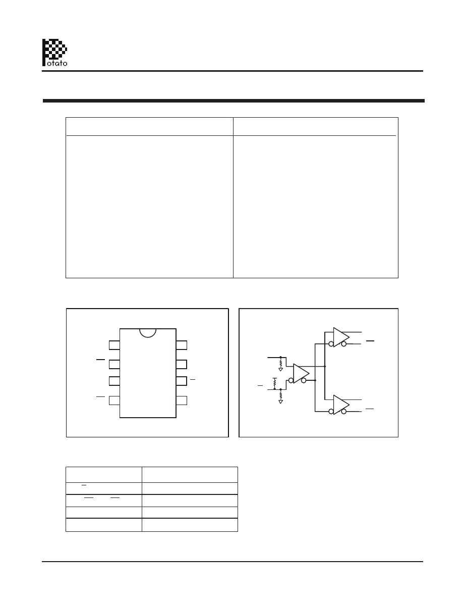
Pin Configuration
Logic Block Diagram
Pin Description
DESCRIPTION:
Potato Semiconductor’s PO100HSTL11A is
designed for world top performance using
submicron CMOS technology to achieve 1.24GHz
HSTL output frequency with less than 2.0ns
propagation delay.
The
PO100HSTL11A
is a low-skew, 1-to-2
differential fanout buffer targeted to meet the
requirements of high-performance clock and data
distribution applications. The device has a fully
differential internal architecture that is optimized
to achieve low signal skews at operating frequen-
cies of up to 1.24GHz .
Vcc
D
D
D
GND
Q0
Q0
Q0
Q1
Q1
Q1
1
2
3
4
8
7
6
5
PIN
D, D
Q0, Q0, Q1, Q1
HSTL Outputs
FUNCTION
LVDS LVPECL HSTL Inputs
V
CC
GND
Ground Supply
Positive Supply
Q0
Q1
D
• Patented Technology
• Two HSTL differential outputs
• One pair of LVDS/LVPECL/HSTL/ differential
or single-ended inputs
• Operating frequency up to 1.24GHz with 2pf load
• Operating frequency up to 900MHz with 5pf load
• Operating frequency up to 400MHz with 15pf load
• Very low output pin to pin skew < 40ps
• Propagation delay < 2.0ns max with 15pf load
• 2.3V to 3.6V power supply
• Industrial temperature range: –40°C to 85°C
• Available in 8-pin SOIC package
• Available in 8-pin TSSOP package
2.3V - 3.6V 1 to 2 Differential Clock/Data Fanout Buffer
1.24GHz Noise Cancellation TTL/CMOS Potato Chip
1
01/01/10
Potato Semiconductor Corporation
PO100HSTL11A
www.potatosemi.com