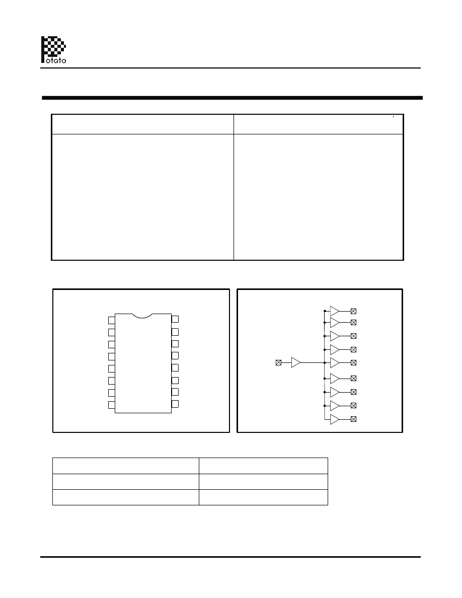
Pin Configuration
Logic Block Diagram
OUTPUT2
OUTPUT3
OUTPUT4
OUTPUT5
OUTPUT6
OUTPUT7
OUTPUT8
OUTPUT9
OUTPUT1
1
2
3
4
5
6
7
8
9
10
11
12
13
14
15
16
BUF_IN
BUF_IN
BUF_IN
OUTPUT1
OUTPUT2
V
DD
V
DD
GND
OUTPUT3
OUTPUT4
OUTPUT 1 to OUTPUT 9
V
DD
OUTPUT9
OUTPUT8
OUTPUT7
GND
OUTPUT6
OUTPUT5
GND
Pin Description
FEATURES:
. Operating frequency up to 700MHz with 2pf load
. Operating frequency up to 550MHz with 5pf load
. Operating frequency up to 350MHz with 15pf load
. Operating frequency up to 100MHz with 50pf load
. Very low output pin to pin skew < 100ps
. Very low pulse skew < 200ps
. VCC = 1.2V to 3.6V
. Propagation delay < 1.9ns max with 15pf load
. Low input capacitance: 3pf typical
. 1:9 fanout
. Available in 16pin 150mil wide SOIC package
. Available in 16pin 173mil wide TSSOP package
Potato Semiconductor’s
PO74G2309A
is
designed for world top performance using
submicron
CMOS
technology
to
achieve
700MHz output frequency with less than 100ps
output pin to pin skew.
PO74G2309A is a 1.2V to 3.6V CMOS
1 input to 9 Output Buffered Driver to
achieve 700MHz output frequency.
Typical applications are clock and signal distribution.
Inputs can be driven from either 3.3V or 5V devices.
This feature allows the use of these devices as
translators in a mixed 3.3V/5V system environment.
. Patented technology
DESCRIPTION:
Pin Name
Description
t
u
p
n
I
Outputs
1.2V - 3.6V 1:9 CMOS Clock Buffered Driver
700MHz TTL/CMOS Potato Chip
1
01/01/10
Potato Semiconductor Corporation
PO74G2309A
www.potatosemi.com