. Patented Technology
. Two HSTL differential outputs
. Two single LVTTL/LVCMOS inputs
. Operating frequency up to 300MHz with 15 pf load
. Very low output pin to pin skew < 30ps
. 3.2-ns propagation delay (max)
. 2.4V to 3.6V power supply
. Industrial temperature range: –40°C to 85°C
. 14-pin TSSOP package
The PO74HSTL85352A is a low-skew, 1-to-2 differential
fanout buffer targeted to meet the requirements of
high-performance clock and data distribution applications.
The device is implemented on CMOS technology and has
a fully differential internal architecture that is optimized to
achieve low signal skews at operating frequencies of up to
300MHz .
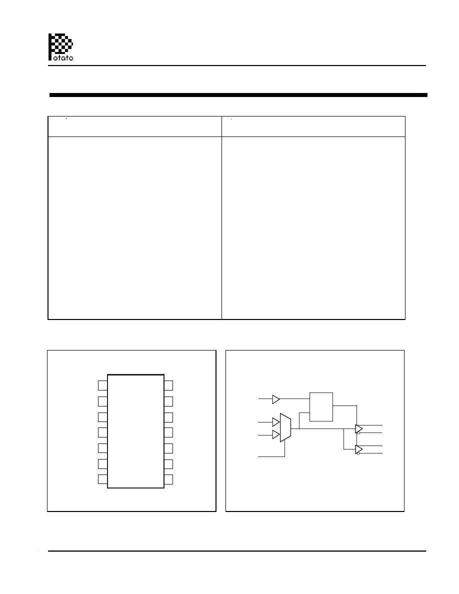
The device features two single-ended input paths that are
multiplexed internally. This mux is controlled by the
CLK_SEL pin. The PO74HSTL85352A functions as a
signal-level translator and fanout on LVCMOS / LVTTL
single-ended signal to two pair of HSTL differential loads.
Since the PO74HSTL85352A introduces negligible jitter
to the timing budget, it is the ideal choice for distributing
high frequency, high precision clocks across back-planes
and boards in communication systems.
FEATURES:
Pin Configuration
Logic Block Diagram
DESCRIPTION:
CLK0
CLK1
Q0
nQ0
Q1
nQ1
0
1
CLK_EN
CLK_SEL
D
Q
LE
V
EE
CLK_EN
CLK_SEL
CLK0
V
EE
CLK1
V
CC
1
2
3
4
5
6
7
14
13
12
11
10
9
8
V
CC
Q0
nQ0
nc
Q1
nQ1
V
CC
LVCMOS Input to HSTL Output 1:2 Fanout Buffer
1
01/01/10
Potato Semiconductor Corporation
PO74HSTL85352A
www.potatosemi.com
300MHz TTL/CMOS Potato Chip