Description
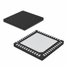
Microsemi A3P030-QNG48 IC FPGA – Field Programmable Gate Array ProASIC3 FPGA ProASIC®3 Family 30K Gates 231MHz 130nm (CMOS) Technology 1.5V 48-Pin QFN EP
Manufacturer: Microsemi
Product Category: FPGA – Field Programmable Gate Array
RoHS: RoHS Compliant Details
Product: A3P030
Number of Logic Elements: 330
Number of Logic Array Blocks – LABs: –
Number of I/Os: 81 I/O
Operating Supply Voltage: 1.5 V
Maximum Operating Temperature: + 70 C
Mounting Style: SMD/SMT
Package / Case: QFN-48
Brand: Microsemi
Maximum Operating Frequency: 231 MHz
Minimum Operating Temperature: 0 C
Number of Gates: 30000
Operating Supply Current: 2 mA
Packaging: Tray
Tradename: Actel
ProASIC3, the third-generation family of Microsemi flash FPGAs, offers performance, density, and features beyond those of the ProASICPLUS family. Nonvolatile flash technology gives ProASIC3 devices the advantage of being a secure, low power, single-chip solution that is Instant On. ProASIC3 is reprogrammable and offers time-to-market benefits at an ASIC-level unit cost. These features enable designers to create high-density systems using existing ASIC or FPGA design flows and tools. ProASIC3 devices offer 1 kbit of on-chip, reprogrammable, nonvolatile FlashROM storage as well as clock conditioning circuitry based on an integrated phase-locked loop (PLL). The A3P015 and A3P030 devices have no PLL or RAM support. ProASIC3 devices have up to 1 million system gates, supported with up to 144 kbits of true dual-port SRAM and up to 300 user I/Os. ProASIC3 devices support the ARM Cortex-M1 processor.
Key Features
High Capacity
15 k to 1 M System Gates
Up to 144 kbits of True Dual-Port SRAM
Up to 300 User I/Os
Reprogrammable Flash Technology
130-nm, 7-Layer Metal (6 Copper), Flash-Based CMOS Process
Instant On Level 0 Support
Single-Chip Solution
Retains Programmed Design when Powered Off
High Performance
350 MHz System Performance
In-System Programming (ISP) and Security
FlashLock® to Secure FPGA Contents
Low Power
Core Voltage for Low Power
Support for 1.5 V-Only Systems
Low-Impedance Flash Switches
High-Performance Routing Hierarchy
Segmented, Hierarchical Routing and Clock Structure
Advanced I/O
700 Mbps DDR, LVDS-Capable I/Os (A3P250 and above)
1.5 V, 1.8 V, 2.5 V, and 3.3 V Mixed-Voltage Operation
Wide Range Power Supply Voltage Support per JESD8-B, Allowing I/Os to Operate from 2.7 V to 3.6 V
Bank-Selectable I/O Voltages—up to 4 Banks per Chip
Single-Ended I/O Standards: LVTTL, LVCMOS 3.3 V / 2.5 V / 1.8 V / 1.5 V, 3.3 V PCI / 3.3 V PCI-X† and LVCMOS 2.5 V / 5.0 V Input
Differential I/O Standards: LVPECL, LVDS, B-LVDS, and M-LVDS (A3P250 and above)
I/O Registers on Input, Output, and Enable Paths
Hot-Swappable and Cold Sparing I/Os
Programmable Drive Strength
Weak Pull-Up/-Down
IEEE 1149.1 (JTAG) Boundary Scan Test
Pin-Compatible Packages across the ProASIC3 Family
ARM Processor Support in ProASIC3 FPGAs
M1 ProASIC3 Devices—ARM®Cortex™-M1 Soft Processor Available with or without Debug
Technical Attributes
Manufacturer:Microsemi
Datasheet:MSCO-S-A0001801885-1.pdf


