Description
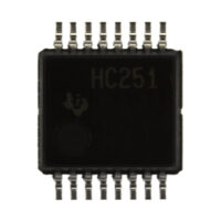
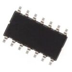
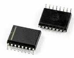
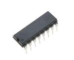
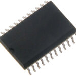
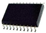
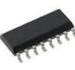
MC74HC646DW Motorola Octal Tri-State Bus Transceiver 2-6V 500mW Surface Mount SMD SOIC-24
The MC54/74HC646 is identical in pinout to the LS646. The device inputs are compatible with standard CMOS outputs; with pullup resistors, they are compatible with LSTTL outputs
Output Drive Capability: 15 LSTTL Loads
•
Outputs Directly Interface to CMOS, NMOS, and TTL
•
Operating Voltage Range: 2 to 6 V
•
Low Input Current: 1
µ
A
•
High Noise Immunity Characteristic of CMOS Devices
•
In Compliance with the Requirements Defined by JEDEC Standard
No. 7A
•
Chip Complexity: 780 FETs or 195 Equivalent Gates
The MC54/74HC646 is identical in pinout to the LS646. The device inputs are compatible with standard CMOS outputs; with pullup resistors, they are compatible with LSTTL outputs. These devices are bus transceivers with D flipflops. Depending on the status of the DataSource Selection pins, data may be routed to the outputs either from the flipflops or transmitted realtime from the inputs (see Function Table and Application Information). The Output Enable and the Direction pins control the transceiver’s function. Bus A and Bus B cannot be routed as outputs to each other simultaneously, but can be routed as inputs to the A and B flipflops. Also, the A and B flipflops can be routed as outputs to Bus A and Bus B. Additionally, when either or both of the ports are in the highimpedance state, these I/O pins may be used as inputs to the D flipflops for data storage. The user should note that because the clocks are not gated with the Direction and Output Enable pins, data at the A and B ports may be clocked into the storage flipflops at any time. Output Drive Capability: 15 LSTTL Loads Outputs Directly Interface to CMOS, NMOS, and TTL Operating Voltage Range: 6 V Low Input Current: 1 µA High Noise Immunity Characteristic of CMOS Devices In Compliance with the Requirements Defined by JEDEC Standard No. 7A Chip Complexity: 780 FETs or 195 Equivalent Gates
Manufacturer:Motorola
Datasheet:Motorola/MC74HC646N.pdf
